ABSTRACT
There is an increasing demand for freeform stretchable display technologies capable of overcoming spatial limitations in next-generation platforms such as augmented reality (AR) and virtual reality (VR). To realize such stretchable displays, all constituent materials—including semiconductors, electrodes, insulators, and substrates—must exhibit sufficient mechanical elasticity. To date, stretchable gate insulators have primarily relied on organic polymers such as poly(4-vinylphenol-co-methyl methacrylate) (PVP-co-PMMA). However, their practical application is significantly limited by poor electrical properties, including low dielectric constant and instability. In this work, we propose a novel gate insulator structure that minimizes the use of solution-based processes, which often suffer from poor uniformity and may damage underlying layers during fabrication. The proposed structure integrates the advantages of both organic and inorganic materials by employing a hybrid configuration. Specifically, high-k HfO2 thin films are deposited on both the top and bottom of an organic layer composed of PVP-co-PMMA, poly(melamine-co-formaldehyde) (PMF) as a crosslinking agent, and propylene glycol monomethyl ether acetate (PGMEA) as a solvent. This inorganic–organic–inorganic structure effectively compensates for the inherent electrical limitations of organic materials. As a result, the fabricated thin-film transistors (TFTs) exhibit improved electrical performance and reliability compared to devices employing a single organic gate insulator.
-
KEYWORDS: Stretchable displays, Gate dielectric, Oxide, Transistors, PvP-co-PMMA, HfO2
1 Introduction
The development of freeform displays, including flexible and stretchable displays, is becoming increasingly important for next-generation technologies such as mobile devices, augmented reality (AR), virtual reality (VR), and bio-integrated systems [
1-
3]. To realize such systems, all components of the display —including semiconductors, electrodes, insulators, and substrates — must exhibit mechanical flexibility and stretchability. Organic materials such as poly(4-vinylphenol-co-methyl methacrylate) (PVP-co-PMMA) have been widely used as flexible gate insulators due to their mechanical compliance [
4–
8]. However, their application is limited by poor electrical properties, including low dielectric constant and instability. Moreover, while flexible substrates (e.g., PDMS laminated with polyimide (PI)) have been explored, prior studies primarily focus on substrate design without proposing a complete device architecture suitable for stretchable displays.
Additionally, thin-film transistor (TFT) devices used as backplanes must be fabricated on flexible substrates in order to achieve flexible and stretchable displays. There are few reports of previous studies in which the gate insulator layer of TFT devices was fabricated using a solution process, despite the fact that a considerable number of studies have previously reported on the electrical characteristics of TFT devices using oxide semiconductors as the channel layer based on solution processes [
9,
10]. In this study, we propose a hybrid inorganic–organic–inorganic (IOI) gate insulator structure that combines the electrical advantages of inorganic materials with the mechanical flexibility of organic materials. By minimizing reliance on solution-based processes—which often suffer from poor reproducibility and potential damage to underlying layers — we demonstrate improved electrical performance and reliability in oxide thin-film transistors (TFTs).
2 Device Design and Fabrication
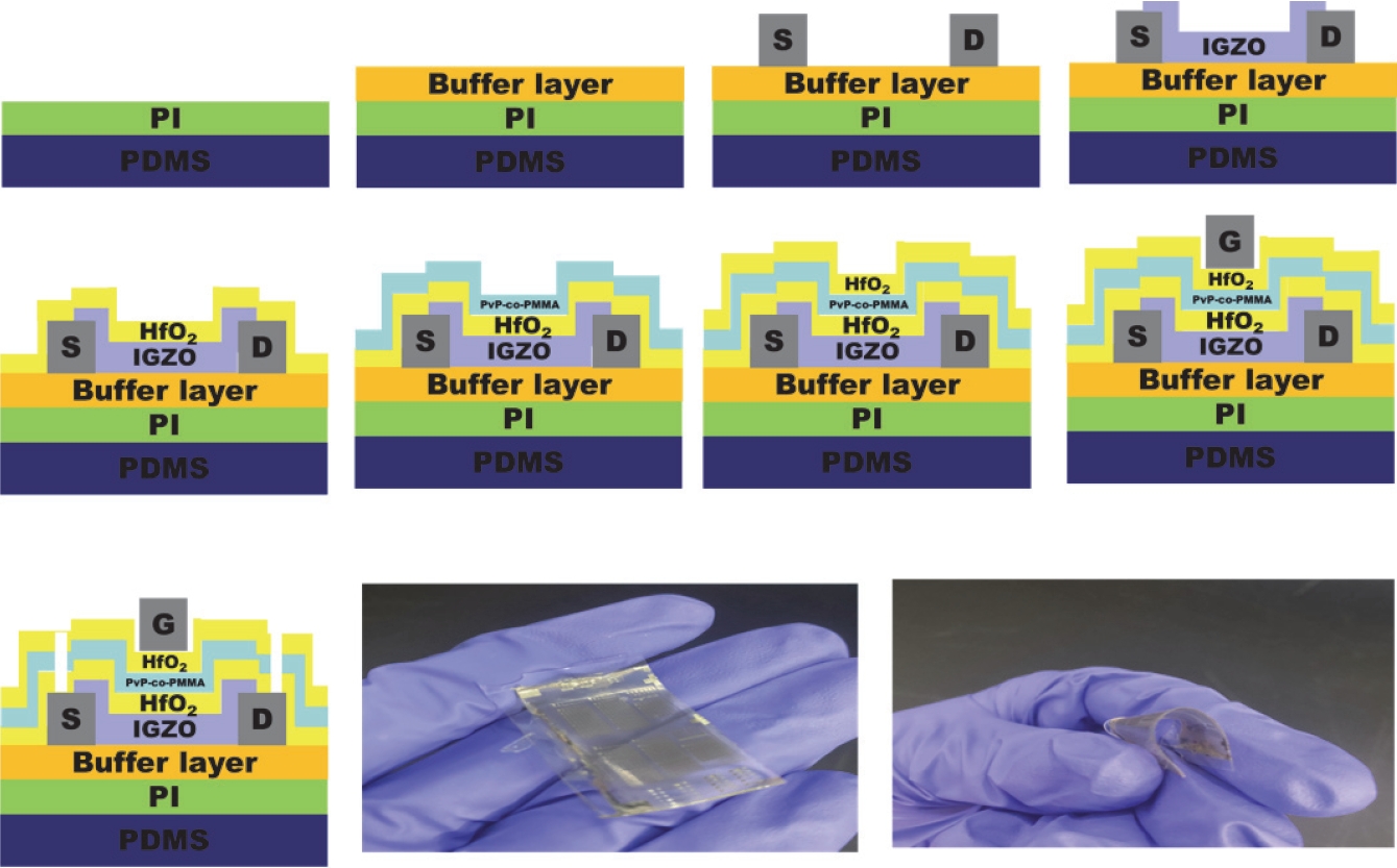
To realize stretchable oxide TFTs, a composite elastic substrate was fabricated by stacking a polyimide (PI) layer onto a polydimethylsiloxane (PDMS) layer, as illustrated in
Fig. 1. The PI layer provides mechanical rigidity, while PDMS contributes high elasticity. This combination enables both structural stability and stretchability. The fabrication process begins with a sacrificial substrate, onto which the PI layer is deposited. After removing the sacrificial substrate, PDMS is formed beneath the PI layer. A buffer layer is subsequently introduced on top of the PI surface to protect the substrate and ensure stable device fabrication. A 100 nm thick HfO₂ layer was deposited using atomic layer deposition (ALD) at 150°C. Source and drain electrodes were then formed by sputtering 200-nm-thick molybdenum (Mo) layers. Subsequently, a 20-nm-thick indium-gallium-zinc oxide (IGZO) semiconductor layer was deposited via plasma-enhanced ALD (PEALD).
3 Gate Insulator Engineering
The gate insulator in this study was a triple-layer structure composed of an organic layer (PVP-co-PMMA (50 um)), a top inorganic layer (HfO2, 10 nm), and a bottom inorganic layer (HfO2, 15 nm). We'll go into more depth on the particular process for manufacturing the gate insulating layer. To create a lower inorganic layer, HfO₂ is first deposited using ALD process on the whole top surface of the semiconductor layer, source, and drain metal layers. To avoid harming the IGZO semiconductor layer created below, the deposition temperature in this method is adjusted to 150°C. The thickness of the lower inorganic layer is formed to a thickness of 25 nm.
The bottom inorganic layer is then covered with an organic layer by spin-coating and curing procedures. Below is a detailed description of the particular process used to generate the organic layer. PvP-co-PMMA (4 weight percent), PGMEA (propylene glycol monomethyl ether acetate) 5 mL, and PMF (poly-methoxy flavones) (4 weight percent) are first combined. At 75°C and atmospheric pressure, the mixture is agitated for 12 hours. The organic layer, which is made up of PvP-co-PMMA, is made better by this stirring procedure. In particular, raising the stirring temperature eliminates moisture, which lowers viscosity. The cross-linking reaction becomes more uniform when the viscosity is reduced. When used as a gate insulating layer, increasing the cross-linking reaction's homogeneity successfully stops leakage current. Propylene glycol and methanol are produced during the hydrolysis of PGMEA, which is utilized as a solvent and includes ester linkages.
Substances with OH groups may be formed as a result of this mechanism. The gate insulating film's roughness may be increased by water or OH groups. MgSO4 was added to reduce the effects of water and OH groups, preventing an increase in the organic layer's roughness. In this case, 2 weight percent of MgSO₄ 4.78 g can be added to the 98-weight percent mixture of the previously mentioned blend (PvP-co-PMMA, PGMEA (propylene glycol monomethyl ether acetate), and PMF (poly-methoxy flavones). Since MgSO4's only function is to react with water molecules to precipitate water, the precise amount of MgSO4 supplied is not important; consequently, MgSO4 can be combined with 1–99 weight percent of the mixture. It was confirmed that the roughness was 0.170 nm with MgSO₄ and 0.203 nm without it. The mixture was then deposited onto the upper surface of the bottom inorganic layer after being filtered to remove contaminants. For this coating procedure, spin coating is an option. The solution was pre-filtered using a 0.2 μm syringe filter in preparation for the spin-coating procedure. The spin-coating process was subsequently carried out for about 30 seconds at speeds of 500, 1,000, and 1,500 RPM, according to the order, after the substrate was set on the spin coater and the solution was dispensed. The organic layer was then created by pre-baking for ten minutes at 100°C, UV treatment for ten minutes, and annealing for three hours at 150°C.
The homogeneity of the cross-linking process is improved by increasing the stirring temperature to 75°C, which lowers the viscosity of the reactants (PMF: PvP-co-PMMA: PGMEA). As a result, leakage current in the gate insulating layer can be effectively controlled. Ester bonds are present in PGMEA, a solvent. Propylene glycol and methanol are produced when PGMEA hydrolyzes, and it's possible that compounds with OH groups will also be created. In this experiment, MgSO
4 was added to eliminate the H
2O and OH groups that can increase the roughness of the gate insulating film, and it was confirmed that they were successfully removed as shown in
Table 1. Improvement of PvP-co-PMMA film quality according to stirring temperature and moisture removal were verified.
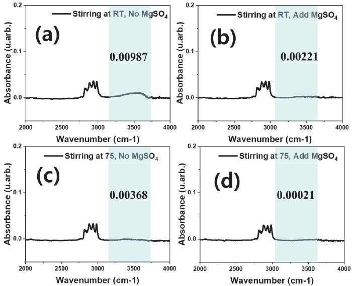
Graphs of the Fourier transform infrared (FT-IR) spectroscopy results for a number of experimental cases are displayed in
Fig. 2. The results for stirring at room temperature without adding MgSO₄ are shown in
Fig. 2(a); the results for stirring at room temperature with MgSO₄ added are shown in
Fig. 2(b); the results for stirring at 75°C without adding MgSO₄ are shown in
Fig. 2(c); and the results for stirring at 75°C with MgSO₄ added are shown in
Fig. 2(d). The current invention's process conditions are shown in
Fig. 2(d). It is proven that when MgSO₄ was added at room temperature (
Fig. 2(b)), the OH peak (3100–3700) was reduced to about one-fourth of what was seen when MgSO₄ was not introduced at room temperature (
Fig. 2(a)). Additionally, when MgSO
4 is not supplied at 75°C, the peak is reduced by about one-third (
Fig. 2(c)), but when MgSO
4 is introduced at 75°C, it is reduced by a factor of 47. Both the reactant concentration and the thin film's roughness are impacted by this variation.
The organic layer was followed by the formation of an upper inorganic layer. The higher inorganic layer shared the same thickness and creation process as the lower inorganic layer. The gate insulator used in this work was a layered structure made up of an organic layer, an upper inorganic layer, and a lower inorganic layer. A single inorganic layer is the most effective way to obtain the electrical characteristics of semiconductor devices, according to experimental confirmation; nevertheless, this layer is insufficient to meet the tensile strength requirements of flexible devices. In order to guarantee tensile strength, a bilayer structure with an organic layer at the bottom and an inorganic layer at the top may be taken into consideration. However, when the organic material came into contact with the semiconductor layer, the device's electrical properties declined. A bottom inorganic layer, an organic layer, and a top inorganic layer make up the triple-layer gate insulator construction we presented in this study. We verified that this structure not only guarantees tensile strength but also keeps the organic layer away from the semiconductor layer, preventing the electrical properties of the device from deteriorating.
Using a traditional single PI layer makes it challenging to achieve a stretchable display, which needs strong elasticity in both the vertical and horizontal planes. A highly elastic PDMS layer was put underneath the traditional PI substrate to solve this. Additionally, an organic PvP-co-PMMA insulating film was coated in between an inorganic HfO
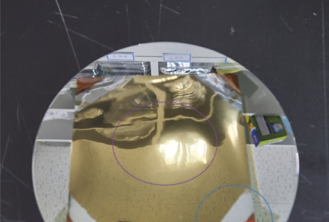
2 insulating film that was produced on both the top and bottom surfaces using atomic layer deposition (ALD) at a low process temperature of 150°C or less. As seen in
Fig. 3 below, increasing the ALD deposition temperature to 250°C causes the PI film to wrinkle, which is why we restricted the ALD deposition temperature for the HfO₂ thin-films to 150°C or below. This resulted in the development of a hybrid organic-inorganic insulating film structure that was stretchable at low process temperatures. The gate insulating film for TFT devices was subsequently used. Following the formation of the gate insulator, a 200-nm-thick layer of molybdenum metal was sputter-deposited on top of it and then patterned to create the gate metal layer.
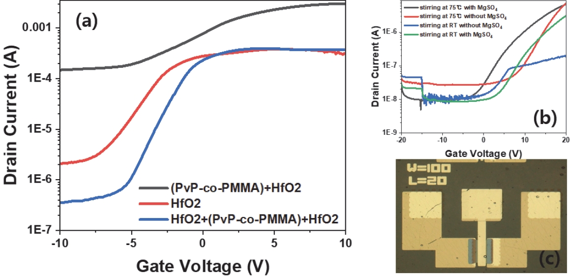
The electrical characteristics of a single-layer HfO₂ gate insulator, a PvP-co-PMMA and HfO₂ double-layer gate insulator, and the triple-layer gate insulator of the oxide TFTs compared in
Fig. 4. While TFT devices with a single HfO₂ gate insulator exhibit the best electrical characteristics (such as subthreshold swing (S.S.) and I
ON/OFF), they do not meet the tensile strength requirements for stretchable TFTs. In the case of a PvP-co-PMMA and HfO₂ double-gate insulator, it has been confirmed that the organic material comes into contact with the oxide semiconductor layer, degrading the semiconductor characteristics. Accordingly, it has been confirmed that depositing inorganic materials such as HfO₂ above and below the organic material improves the device’s electrical characteristics while also ensuring tensile strength.
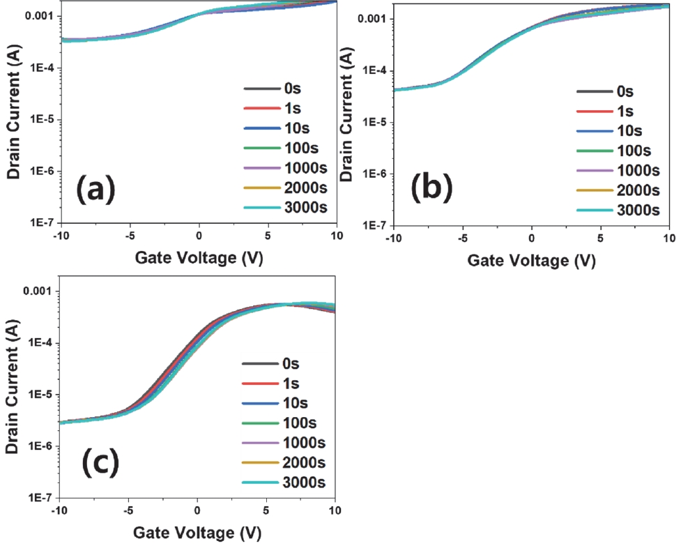
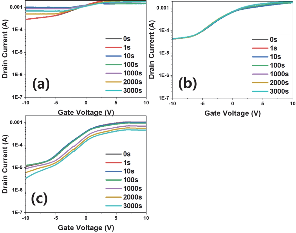
The electrical reliability of oxide TFT devices with three different gate dielectric structures has been evaluated in addition to their electric characteristics. The transfer characteristics (I
DS-V
GS) of oxide TFTs with different three gate insulator structures under a positive gate bias (10 V) are shown in
Fig. 5, while those under a negative gate bias (-10 V) are presented in
Fig. 6. The oxide semiconductor layer in contact with the organic layer was responsible for the observable deterioration and conductive behavior in the bilayer structure, while the triple-layer structure showed a positive shift phenomenon instead of the usual negative bias stability behavior. Consequently, it was verified that the HfO₂–PvP-co-PMMA–HfO₂ triple-layer structure suggested in this work had advantageous transfer characteristics. This implies that the organic layer treatment minimizes performance degradation by preventing leakage current production.
4 Conclusion
This study presents a hybrid inorganic–organic–inorganic gate insulator for stretchable oxide TFTs. Key findings include: In first, we stirred at 75°C instead of room temperature improves the crosslinking reaction's homogeneity and yield by reducing the viscosity of the reactants. Additionally, the addition of moisture-absorbing MgSO4 improves the on-, off-current and subthreshold swing (S.S.) values of the oxide TFT devices by removing impurities from the gate insulator and reducing the roughness of the thin film. Based on this, the electrical characteristics were assessed when a hybrid structure with both organic and inorganic layers was used to create the gate insulator while keeping the stirring conditions at 75°C and adding MgSO4. Consequently, an inorganic-organic-inorganic triple-layer structure was suggested, which guarantees superior tensile strength in comparison to a single HfO₂ layer and reduces the oxide semiconductor layer degradation brought on by organic materials when utilizing a PvP-co-PMMA and HfO₂ double-layer structure. This study is important because it addresses the leakage current problem that occurs when employing an organic single-layer gate insulator, even though the electrical characteristics are not as good as those of devices using an inorganic single-layer gate insulator. The gate insulator structure used in this work is a multilayer structure of organic and inorganic insulating films created at comparatively low processing temperatures. In doing so, it creates a stretchable gate insulator that makes it possible for semiconductor devices to have extremely dependable stretchable architectures. Additionally, this approach has the potential to be used in the bio-industry, augmented-, virtual-reality (AR/VR) displays, and future next-generation mobile devices by altering the substrate structure to accommodate the high degree of stretchability required in both vertical and horizontal directions for stretchable displays.
Notes
-
Acknowledgement
This work was supported by the Academic Promotion System Tech University of Korea.
-
Conflict of Interest
The author(s) (Sung-Hwan Choi) currently serves on the editorial board of JEEM, but was not involved in any part of the publication process. Other than this, the authors declare that they have no relevant potential conflicts of interest.
-
Author Contributions
Chae Yeon Kim: Writing - Original Draft, Conceptualization, Validation, Formal analysis.
Sung-Hwan Choi: Writing - Original Draft, Writing - Review & Editing, Visualization, Supervision, Project administration, Funding acquisition.
Data Availability
Data available on request from the authors.
Fig. 1.Cross-sectional schematic of a stretchable thin-film semiconductor device during fabrication
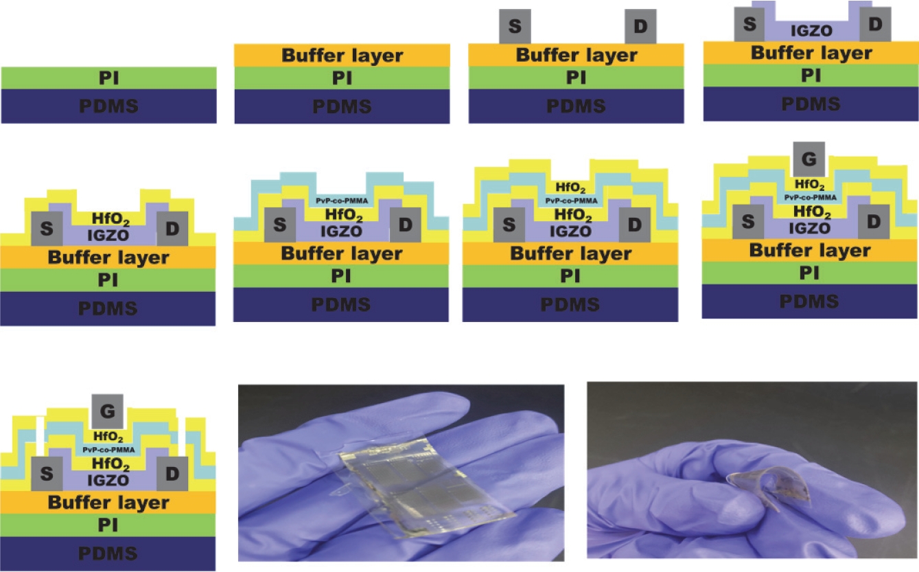
Fig. 2.FT-IR characteristics of (a) stirring at room temperature (RT) without MgSO4, (b) stirring at RT with MgSO4, (c) stirring at 75°C without MgSO4, and (d) stirring at 75°C with MgSO4
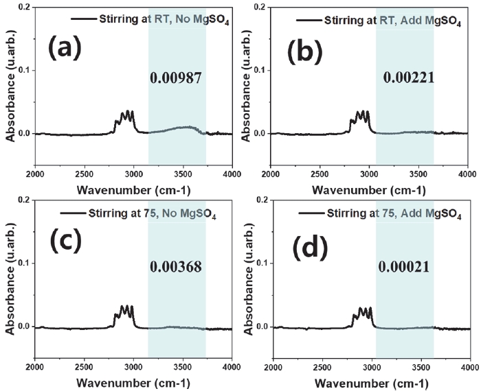
Fig. 3.A PI layer that has been bonded to the top of a 6-inch wafer warps when the ALD process is performed at a substrate temperature of 250°C (Gate insulators: HfO2 thin-films)
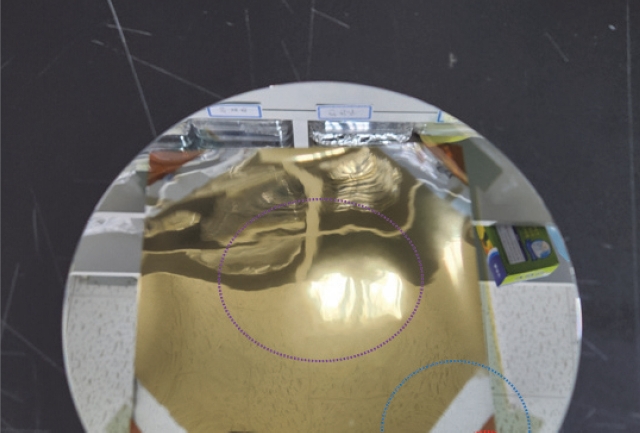
Fig. 4.Transfer characteristics of (a) oxide TFTs with single-, double-, and triple-layer gate insulators, (b) different stirring conditions on silicon wafers; and (c) optical microscope image of stretchable oxide TFTs. The electrical properties of a single-layer HfO2 gate insulator, a doublelayer gate insulator made of PvP-co-PMMA and HfO2, and a triple-layer gate insulator are compared in this graph
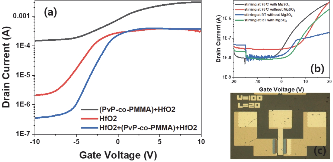
Fig. 5.Transfer characteristics of oxide TFTs using (a) (PvP-co-PMMA)+HfO2, (b) HfO2, and (c) HfO2+PvP-co-PMMA)+HfO2 gate insulators with a positive gate bias applied directly (VGS = +10 V)
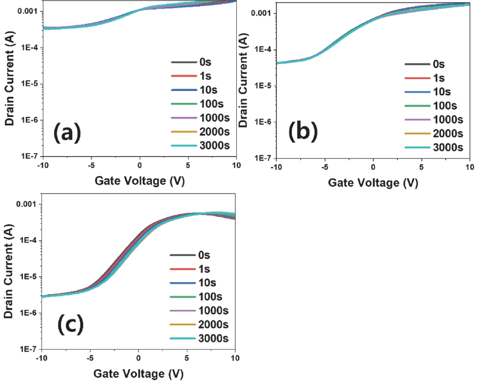
Fig. 6.Transfer characteristics of oxide TFTs using (a) (PvP-co-PMMA)+HfO2, (b) HfO2, and (c) HfO2+PvP-co-PMMA)+HfO2 gate insulators with a negative gate bias applied directly (VGS = -10 V)
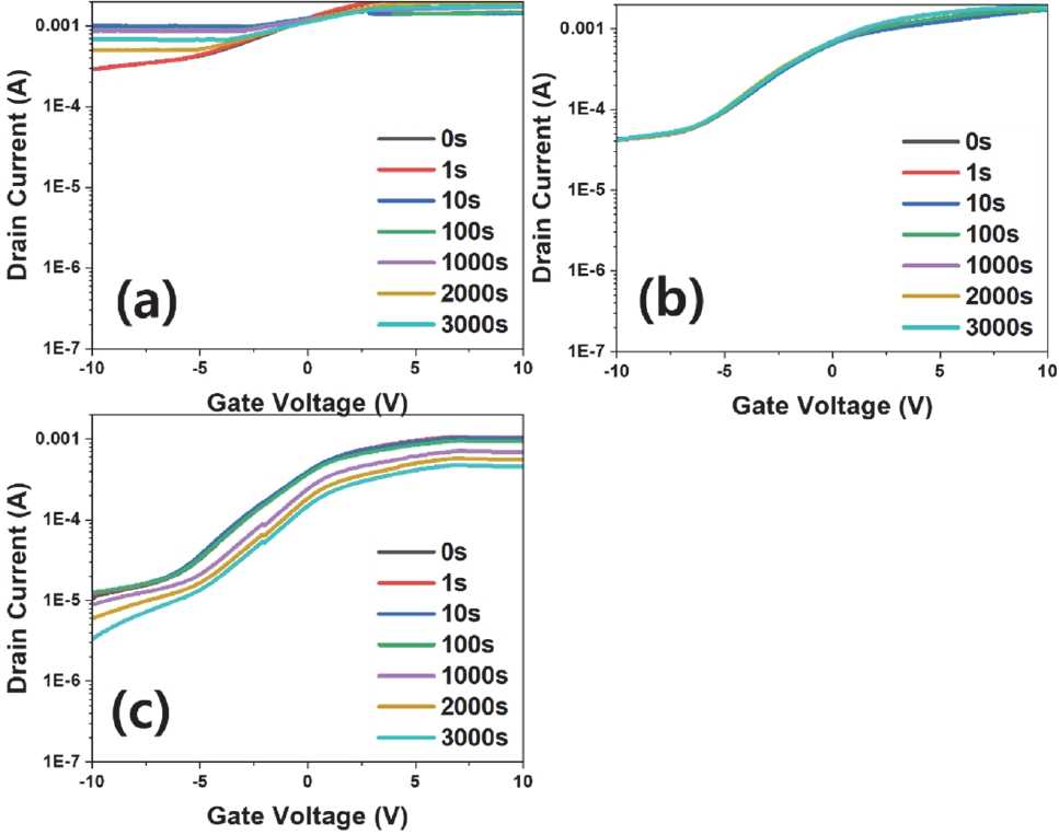
Table 1.Changes in atomic force microscope (AFM) roughness of thin films due to temperature and moisture removal
Table 1.
|
Rq (nm) |
Ra (nm) |
|
Stirring at RT |
0.387 |
0.35 |
|
Stirring at 75°C |
0.278 |
0.221 |
|
Stirring at RT (added MgSO4) |
0.291 |
0.286 |
|
Stirring at 75°C (added MgSO4) |
0.203 |
0.17 |
References
- 1. K. L. Han, W. B. Lee, Y. D. Kim, J. H. Kim, B. D. Choi, and J. S. Park, ACS Appl. Electron. Mater., 3, 5037 (2021). doi: https://doi.org/10.1021/acsaelm.1c00806
- 2. M. Y. Kim, H. W. Kim, C. Oh, S. H. Park, and B. S. Kim, ACS Appl. Electron. Mater., 6, 435 (2024). doi: https://doi.org/10.1021/acsaelm.3c01431
- 3. X. Li, M. M. Hasan, H. M. Kim, and J. Jang, IEEE Trans. Electron Devices, 66, 2971 (2019). doi: https://doi.org/10.1109/ted.2019.2918160
- 4. H. J. Cho, D. H. Lee, E. K. Park, M. S. Kim, S. Y. Lee, K. C. Park, H. Choe, J. H. Jeon, and Y. S. Kim, Thin Solid Films, 673, 14 (2019). doi: https://doi.org/10.1016/j.tsf.2019.01.025
- 5. X. Zhang, J. H. Park, S. Baang, J. Park, S. H. Piao, S. H. Kim, and H. J. Choi, J. Korean Phys. Soc., 65, 1956 (2014). doi: https://doi.org/10.3938/jkps.65.1956
- 6. S. Baang, H. Lee, Y. Ham, X. Zhang, J. Park, H. W. Lee, Y. K. Kim, S. H. Piao, and H. J. Choi, J. Korean Phys. Soc., 67, 2124 (2015). doi: https://doi.org/10.3938/jkps.67.2124
- 7. S. H. Piao, H. Lee, J. Park, and H. J. Choi, J. Nanosci. Nanotechnol., 20, 4188 (2020). doi: https://doi.org/10.1166/jnn.2020.17567
- 8. J. S. Hur, J. O. Kim, H. A. Kim, and J. K. Jeong, ACS Appl. Mater. Interfaces, 11, 21675 (2019). doi: https://doi.org/10.1021/acsami.9b02935
- 9. J. Y. Lee, H. S. Kim, and S. J. Kim, J. Korean Inst. Electr. Electron. Mater. Eng., 33, 93 (2020). doi: https://doi.org/10.4313/JKEM.2020.33.2.93
- 10. H. G. Jang, W. K. Kim, M. S. Oh, and S. H. Kwon, J. Korean Inst. Electr. Electron. Mater. Eng., 33, 286 (2020). doi: https://doi.org/10.4313/JKEM.2020.33.4.286