ABSTRACT
This review offers a critical overview of recent developments in lead-free piezoelectric materials and flexible device architectures for self-powered wearable and Internet of Things systems. It examines the scientific and technological rationale for replacing conventional battery-dependent power sources with ambient mechanical energy harvesters, and it evaluates the relative merits of inorganic ceramics, organic polymers, and composite systems in achieving efficient electromechanical conversion under practical operating conditions. The discussion further considers compositional tuning, phase boundary engineering, microstructural optimization, and device-level integration as key strategies for improving piezoelectric output, mechanical compliance, durability, and manufacturability. By connecting fundamental materials design with application-driven device requirements, the review identifies the principal challenges and emerging directions necessary for the realization of reliable, scalable, and sustainable electronic platforms.
-
KEYWORDS: Energy harvesting, Piezoelectric, Self-powered, IoT, Flexible, Wearable
1 Introduction
The escalating global demand for energy, together with accelerating global warming and environmental pollution, has emerged as a critical challenge of the twenty-first century. In parallel, the rapid growth of cloud computing, big data, and artificial intelligence has driven the widespread deployment of Internet of Things (IoT) technologies, profoundly reshaping industrial manufacturing, transportation infrastructures, and personalized healthcare. This digital transformation, however, places stringent demands on power supply, and conventional electrochemical batteries have become a primary bottleneck to the large-scale realization of wearable and distributed electronic systems [
1].
Although individual IoT sensor nodes typically operate at milliwatt or sub-milliwatt power levels, their aggregate energy consumption over densely deployed networks is substantial. Frequent battery replacement or recharging is therefore impractical, particularly in remote, embedded, or otherwise inaccessible locations. Moreover, the finite lifetime, rigid form factors, and non-negligible volume of conventional batteries hinder further miniaturization and conformal integration on soft, curved, or dynamically deforming surfaces. From a sustainability perspective, the large-scale production, recycling, and disposal of batteries raise serious concerns about resource depletion and environmental contamination, standing in stark contrast to the drive toward greener, more sustainable electronic technologies [
2,
3].
These multifaceted constraints have catalysed intensive efforts toward self-powered technologies that harvest ambient energy to support the autonomous operation of low-power electronic systems. Such systems convert ubiquitous energy sources, including solar radiation, thermal gradients, and mechanical motion, into electrical energy using appropriately engineered harvesters, with the output either directly powering devices or intermittently charging integrated storage units. Photovoltaic, thermoelectric, and piezoelectric energy harvesters have been extensively investigated in this context, each based on distinct physical mechanisms and subject to different limitations in environmental dependence, integration complexity, and form factor. While solar and thermoelectric approaches have achieved considerable success, their deployment in wearable and distributed platforms is often constrained by variability in illumination and weather, the need for persistent temperature gradients, and typically rigid or bulky device architectures that limit installation and integration [
4].
By contrast, piezoelectric energy harvesting is especially attractive for wearable, body-integrated, and distributed IoT applications because mechanical energy is abundant in the human body and its immediate environment, is generated continuously during daily activities, and can be accessed locally at the device site. The human body serves as a rich reservoir of mechanical energy, arising from both involuntary physiological processes and voluntary motion. Respiratory movements, cardiac contractions, and blood circulation generate continuous mechanical stimuli. In contrast, joint motions of the ankle, knee, hip, elbow, and shoulder during locomotion and routine tasks provide intermittent yet substantial mechanical inputs. The combined mechanical power associated with processes such as breathing and walking can reach on the order of 0.1–1 W, which is, in principle, sufficient to sustain many low-power wearable and implantable devices when efficiently harvested. Piezoelectric energy harvesting thus offers a fundamental advantage in that it directly transduces dynamic mechanical deformation into electrical signals, enabling self-sustaining wearable systems that can substantially reduce reliance on conventional batteries [
5].
For practical body-integrated operation, however, energy harvesters must be lightweight, mechanically compliant, and able to maintain intimate, stable contact with skin, textiles, or soft substrates under repeated bending, stretching, and complex multiaxial deformation. These mechanical and interfacial requirements have driven the rapid emergence of flexible piezoelectric energy harvesters as a major research focus. Inorganic piezoelectric ceramics offer high piezoelectric coefficients and mature processing, but their intrinsic brittleness and rigidity severely limit their suitability in flexible and conformal formats [
2]. Conversely, organic piezoelectric polymers such as poly (vinylidene fluoride) (PVDF) and its copolymers offer low density, mechanical flexibility, and facile solution processing, yet typically exhibit lower piezoelectric response than their ceramic counterparts [
6]. Composite architectures that embed piezoelectric ceramic fillers within polymer matrices have therefore been widely explored as a promising route to reconcile high electromechanical coupling with the flexibility, durability, and processability required for nextgeneration wearable and body-integrated piezoelectric energy harvesters [
4].
Concurrently, device-level structures and fabrication strategies for flexible piezoelectric energy harvesters have undergone substantial diversification and refinement. Beyond early cantilever-type geometries designed primarily for narrow-band vibration harvesting, recent research now encompasses a broad spectrum of architectures, including multilayer thin-film stacks, interdigitated electrode configurations, serpentine and kirigami-inspired layouts, and fibers or textile-based formats [
7,
8]. These architectures are engineered to enhance mechanical adaptability, maximize effective strain transfer to the active piezoelectric elements, and maintain stable electrical output under complex deformation modes such as bending, stretching, twisting, and compression. In parallel, advances in micro- and nanofabrication, transfer printing, and solution or printing-based deposition techniques have enabled the integration of high-quality piezoelectric layers onto flexible, stretchable, and even bioresorbable substrates, thereby expanding the range of accessible applications [
9].
As a result of these developments, flexible piezoelectric energy harvesters are increasingly recognized as strong candidates for powering next-generation wearable electronics and distributed IoT systems, owing to their high sensitivity to mechanical deformation, favourable energy-conversion characteristics, structural simplicity, and compatibility with scalable manufacturing processes. Their demonstrated potential spans diverse application domains, including wearable health monitoring, self-powered sensing platforms, transportation infrastructure management, aerial systems, and biomedical implants [
10–
12].
In this review, we present a systematic and integrated perspective on recent advances in flexible piezoelectric energy harvesters across two interconnected pillars: (i) piezoelectric materials, encompassing inorganic, organic, and composite systems; (ii) application-driven implementations in wearable, biomedical, and distributed IoT platforms. By explicitly linking materials design and application requirements, this review seeks to clarify key structure-property-performance relationships, articulate the design principles that underpin high-performance flexible piezoelectric harvesters, and delineate persistent challenges and future research directions. Ultimately, these insights are intended to guide the development of reliable, scalable, and truly self-powered flexible electronic systems that advance sustainable energy generation and extend the operational lifetimes of emerging wearable and IoT technologies.
2 Types of Piezoelectric Materials
2.1 Inorganic Materials
2.1.1 Barium Titanate
Barium titanate (BaTiO
3, BTO), a prototypical lead-free ferroelectric perovskite, has re-emerged as a cornerstone material for capacitors, actuators, piezoelectrics, and flexible energy harvesters. This resurgence over the past decade stems from intensive research on composition design, microstructure control, and nano-structuring, positioning BTO-based systems as viable, environmentally compliant alternatives to lead-containing ceramics. BTO crystallizes in the classical ABO
3 perovskite structure and exhibits successive temperature-driven phase transitions (cubic → tetragonal → orthorhombic → rhombohedral) that underpin its ferroelectric and piezoelectric functionality. The spontaneous polarization originates from the off-center displacement of Ti⁴⁺ cations within TiO
6 octahedra, yielding high dielectric permittivity, switchable polarization, and nonlinear electromechanical coupling. Although BTO exhibits a lower Curie temperature and piezoelectric coefficients than PZT benchmarks, its non-toxic composition, mature processing routes, and broad chemical compatibility make it highly attractive for sustainable device applications. Recent progress in the BiTiO
3-based lead-free dielectrics has been driven by targeted microstructural, compositional, and architectural innovations that are exemplified by seminal works achieving progressively higher recoverable energy densities (Wrec) and efficiencies (η). Each advancement builds incrementally, addressing specific bottlenecks like remnant polarization (Pr), low breakdown strength (Eb), and thermal instability [
13,
14].
Glass-modified ferroelectrics marked the initial breakthrough in microstructural control. By inducing liquid-phase sintering, these additives refine grains and densify ceramics, substantially elevating breakdown strength (Eb) without altering intrinsic chemistry. Wang et al. [
15] incorporated 27.68BaCO₃–36.92SrCO₃–29TiO₂– 22SiO₂–12Al₂O₃–2.4BaF₂ glass (7 wt%) into pure BTO, achieving significant grain refinement as a result of the increase in the glass additive concentration. Moreover, it was observed that the breakdown strength-grain size relationship obeyed the expected parabolic trend. Furthermore, the dielectric breakdown strength increased due to decreases in grain size and improvements in charge transport behaviour. Patel et al. [
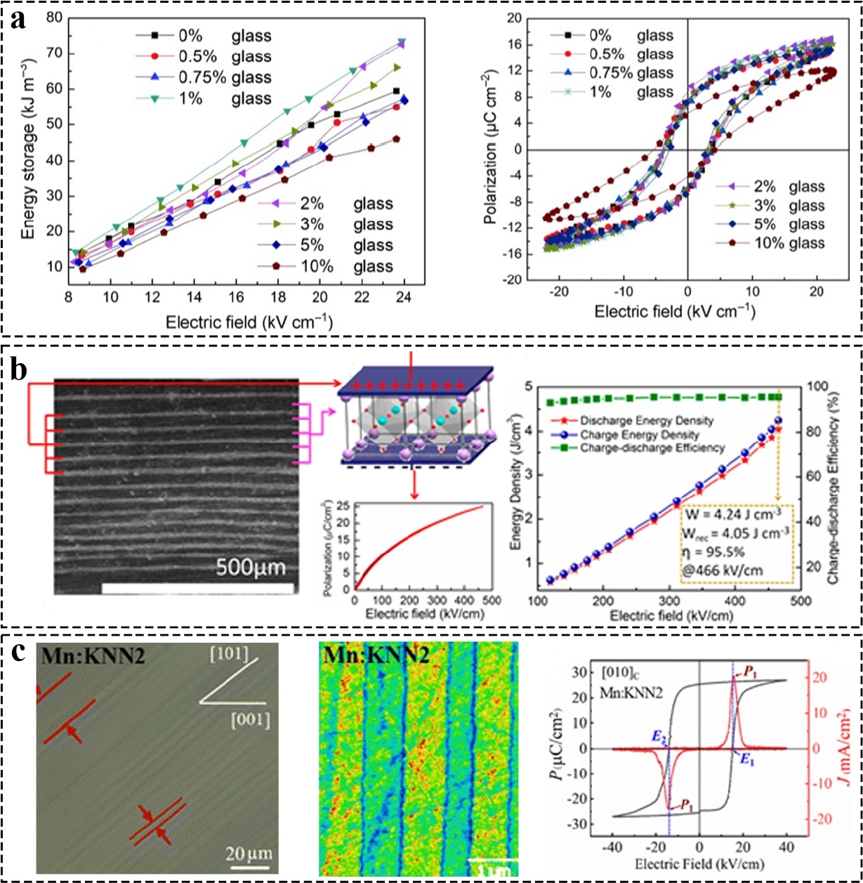
16] extended this to Vdoped BTBO with 3BaO–3TiO₂–B₂O₃ glass (1 wt%), forming insulating boundaries for temperature-invariant loops, which resulted in the improvement of the energy storage (Wrec = 0.0747 J/cm³ at 22 kV/cm). Additionally, the addition of glass enhanced polarization and the temperature -independent performance as shown in
Figure 1(a). Culminating this phase, Yang et al. [
17] demonstrated B₂O₃–Al₂O₃–SiO₂ glass (5 wt%) phase coexistence in BCZT, amplifying Wrec 5.5-fold to 1.153 J/cm³ at 200 kV/cm and unlocking denser, lower-loss microstructures.
Recent studies on compound doping have transitioned BTO from classical ferroelectrics toward slim-loop variants, systematically suppressing remnant polarization (P
r), depressing Curie temperature (TC), and inducing morphotropic phase boundaries (MPBs) or secondary phases for enhanced energy efficiency (η) and breakdown strength (Eb) critical for bridging to full relaxor behavior [
18,
19]. This phase marks a chemical evolution beyond microstructural tweaks, in which lead-free compounds such as MgO, YNbO
4, BiFeO
3, Bi
0.5Na
0.5TiO
3 (BNT), and KNbO
3 are repeatedly combined with BTO to disrupt long-range order while preserving high saturation polarization (P
max). Dong et al. [
20] pioneered YNbO
4 doping (0.07 mol) in BTO, where secondary phase formation suppressed ferroelectric nonlinearity and lowered TC, yielding 0.93BTO–0.07YNbO₄ with Wrec = 0.651 J/cm³ and η = 92%, exemplifying BTO-rich normal ferroelectric optimization limited to modest densities. Liu et al. [
21] advanced acceptor doping with MgO (0.25 wt%), stabilizing dielectric constant (εr) across temperatures for MLCC compatibility while elevating Eb, achieving Wrec = 0.9 J/cm³ (η = 73.3%). Xu et al. [
22] leveraged sol-gel for close-packed grains in (1-x) BTO–BNT–xKNbO
3, where KNbO
3 (x=0.05) minimized Pr and ensured thermal loop stability, delivering ferroelectric-record Wrec = 1.72 J/cm³ at 168 kV/cm.
Relaxor ferroelectrics have also revolutionized BTO performance by inducing polar nanoregions (PNRs) via multi-cation disorder, yielding ultra-slim P–E loops with minimal Pr, high P
max, diffuse phase transitions, and exceptional field/temperature resilience, elevating W
rec from ~1 J/cm³ (ferroelectrics) to 4–8 J/cm³ while maintaining η >90% across 100–300°C [
23–
25]. PNRs shortrange, dynamic clusters disrupting long-range order realign reversibly under fields, minimizing hysteresis loss; non-ergodic states below freezing T are avoided by targeting room-temperature ergodic relaxors [
26]. Huang et al. [
27] Gd-doped (0.15 mol) 0.7BTO–0.3Sr
0.2Bi
0.7TiO
3 (0.2–0.5 μm grains, single perovskite), exploiting rare-earth disorder for broad stability (30–150°C, 10–1,000 Hz; Δεr minimal), achieved Wrec = 3.2 J/cm³ at 330 kV/cm (η = 91.5%). Furthermore, doping BTO with Gd resulted in a ceramic with excellent temperature stability and outstanding frequency stability. Si et al. [
28] engineered 0.88BTO– 0.12Bi(Mg
0.5Sn
0.5)O
3 for Sn/Zr-like B-site mismatch. Using the BMS modification, the grain size of the BT-BMS ceramics was greatly reduced, thereby improving the dielectric breakdown strength. The resulting ceramic delivered η = 94% (Wrec = 2.25 J/cm³ at 240 kV/cm; stable at 55–150°C). Additionally, Hu et al. [
29] showcased a benchmark relaxor study where they induced nano-scale polarization mismatch/reconstruction in 0.6BTO–0.4Bi (Mg
0.5Ti
0.5) O
3, yielding Wrec = 4.49 J/cm³ at 340 kV/cm (η = 93%, stable to 170°C with minimal ΔWrec). Furthermore, the establishment of B-O coupling, a narrow hysteresis loop, and high breakdown strength demonstrated that the BT-BMT relaxor ceramic is a promising lead-free bulk dielectric material for energy-storage capacitor applications. Study by Li et al. [
30] fabricated multilayer 0.90BTO–0.10BiLi
0.5Ta
0.5O
3 whereby the samples were densified at 1,200 degrees, which enabled them to have a high-crystallinity; low sintering T and reduced tan δ, thus attaining Wrec = 4.05 J/cm³ (single-layer 2.2 J/cm³), η = 95.5%, discharge time 0.32 μs, which was ideal for pulsed MLCCs as illustrated in
Figure 1(b). Ogihara et al. [
31] leveraged highactivation BS solubility in 0.7BTO–0.3BiScO₃ for weakly coupled PNRs (X7R to 300°C), achieving Wrec = 6.1 J/cm³ at 730 kV/cm. In another study, Qi et al. [
32] developed a nanodomain engineered 0.33BTO–0.57BiFeO
3–0.1NaNbO
3 bulk ferroelectrics through the integration of a high spontaneous polarization gene-wide band gaps and heterogeneous nanodomain structure. The device generated a record Wrec = 8.12 J/cm³ at 360 kV/cm (η = 90%), with excellent thermal stability up to 25°C. The substitution of NaNbO
3 for BF led to increased band gaps, reduced grain size, and increased resistivity, which together were responsible for the significant improvement in dielectric breakdown strength.
2.1.2 Potassium Sodium Niobate
Potassium sodium niobate (K
1−xNa
xNbO
3, KNN) ceramics have emerged as promising lead-free alternatives to Pb(Zr, Ti)O
3 (PZT) for piezoelectric applications, driven by environmental regulations and demand for biocompatible materials. These materials exhibit perovskite flexibility and polymorphic phase transitions (rhombohedral-orthorhombic-tetragonal), enabling tunable Curie temperatures (TC) [
33–
35]. Key innovations to achieve highquality films include physical vapor deposition (PVD) techniques such as RF magnetron sputtering and pulsed laser deposition (PLD), which enable epitaxial growth on substrates like LaAlO
3 and SrTiO
3, as well as chemical solution deposition (CSD) using excess alkali (≥10 mol% K/Na) and stabilizers (PVP, EDTA) to mitigate volatility and secondary phases [
36–
38]. Saito et al. [
39] pioneered KNN–LiTaO
3–LiSbO
3 (KNN-LTLS) textured ceramics via reactive template grain growth (RTGG) using NaNbO
3 templates, shifting the orthorhombic-tetragonal polymorphic phase transition (PPT, TOT) to near room temperature (~25–40°C from 195°C). This phase convergence enabled easy polarization rotation, yielding d
33=416 pC/N, tripling that of pure KNN and approaching soft PZT, while retaining high TC≈300oC, thereby igniting global lead-free research through chemical pressure tuning. In recent years, Mn doping has been an effective approach to improve the electrical properties of KNN films. It has been reported that the introduction of Mn can effectively reduce the number of both oxygen vacancies and holes, thereby reducing the leakage current in KNN films. A study by Yizhu Sun et al. [
40] demonstrated that using the sol-gel method to deposit Mn-doped KNN improved the ferroelectric photovoltaic effects of the doped KNN films. This was driven by Mn doping, which manipulated the band gap and directly influenced the ferroelectric photovoltaic effect. Both parameters of J
sc and V
oc increased greatly as a result of the improved ferroelectric polarization and the narrowing of the band gap. Yao Zhang et al. [
41] investigated the effect of composition gradient on domain structure and piezoelectric properties in Mn-doped KNN single crystals. They stated that Mn-KNN single crystals grown with a composition gradient using the top-seeded solution growth method exhibited a uniform spontaneous orientation and large macro-piezoelectric properties (83 pC/N). Furthermore, enhancing the piezoelectric performance strengthened the lattice's linear symmetry as demonstrated in
Figure 1(c). Zhang et al. [
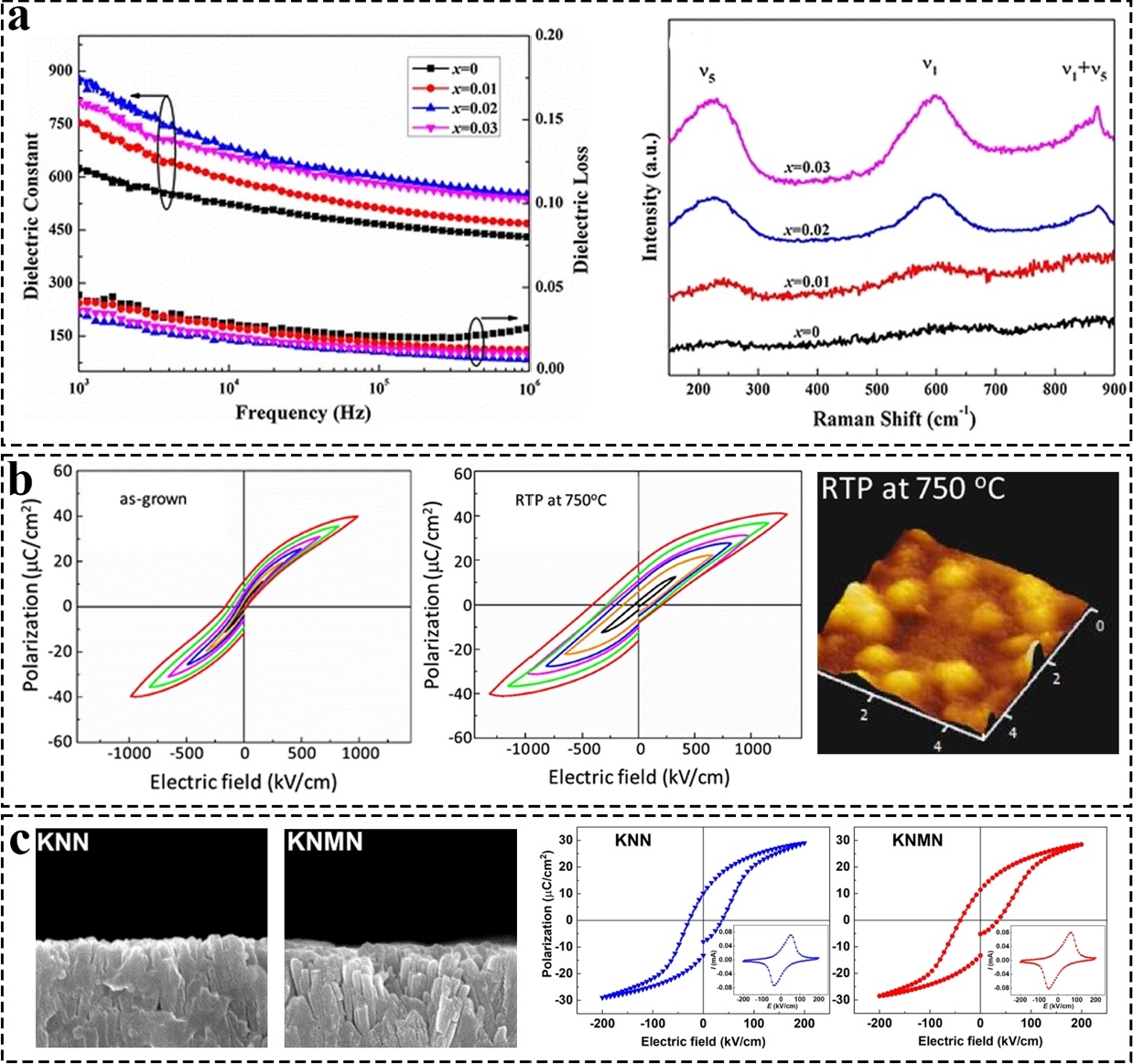
42] developed a high-quality lead-free piezoelectric xMndoped (KNLN, X=0, 0.01, 0.02, 0.03) successfully deposited onto Pt substrates by the sol-gel method. The results showed that 2 mol% Mn-doped KNLN films exhibited better dielectric properties and lower leakage current than the other components. It was evident that KNLN films that had Mn-doping content x of 0.02 had improved dielectric and ferroelectric properties, as shown in
Figure 2(a). Additionally, the films displayed well-saturated ferroelectric P-E hysteresis loops at high applied electric fields. A recent study by Sheeraz et al. [
43] demonstrated the influence of post-annealing on Mn-doped KNN films. They reported that the films were fabricated using RF magnetron sputtering, and that post-annealed samples showed an increased (100) peak intensity, along with the appearance of (200) diffraction, demonstrating the crystalline quality of the post-annealed KNMN film. Furthermore, P-E hysteresis performance improved, along with a reduction in leakage current density, after post-annealing the KNMN film, as represented in
Figure 2(b). The obtained remnant polarization and coercive electric field of the post-annealed samples were 18.8 μc/cm
2.In addition, Phu et al. [
44] enhanced the polarization fatigue behavior of KNN thin films through Mn doping. They demonstrated that the ferroelectric fatigue was significantly suppressed in 0.4 mol% Mn-doped KNN films as compared to the pure KNMN films, as shown in
Figure 2(c). The number of mobile-charged defects decreased in the presence of multivalent Mn dopants, resulting in a decrease in leakage current density. Further, the reduction in charged-defect density weakened the domain-wall pinning effect, thereby suppressing polarization fatigue in KNN films.
Li doping of KNN films has also been extensively studied, with several studies demonstrating that slight lithium doping can improve piezoelectric properties and reduce leakage current in stoichiometric KNN. A study done by Bu et al. [
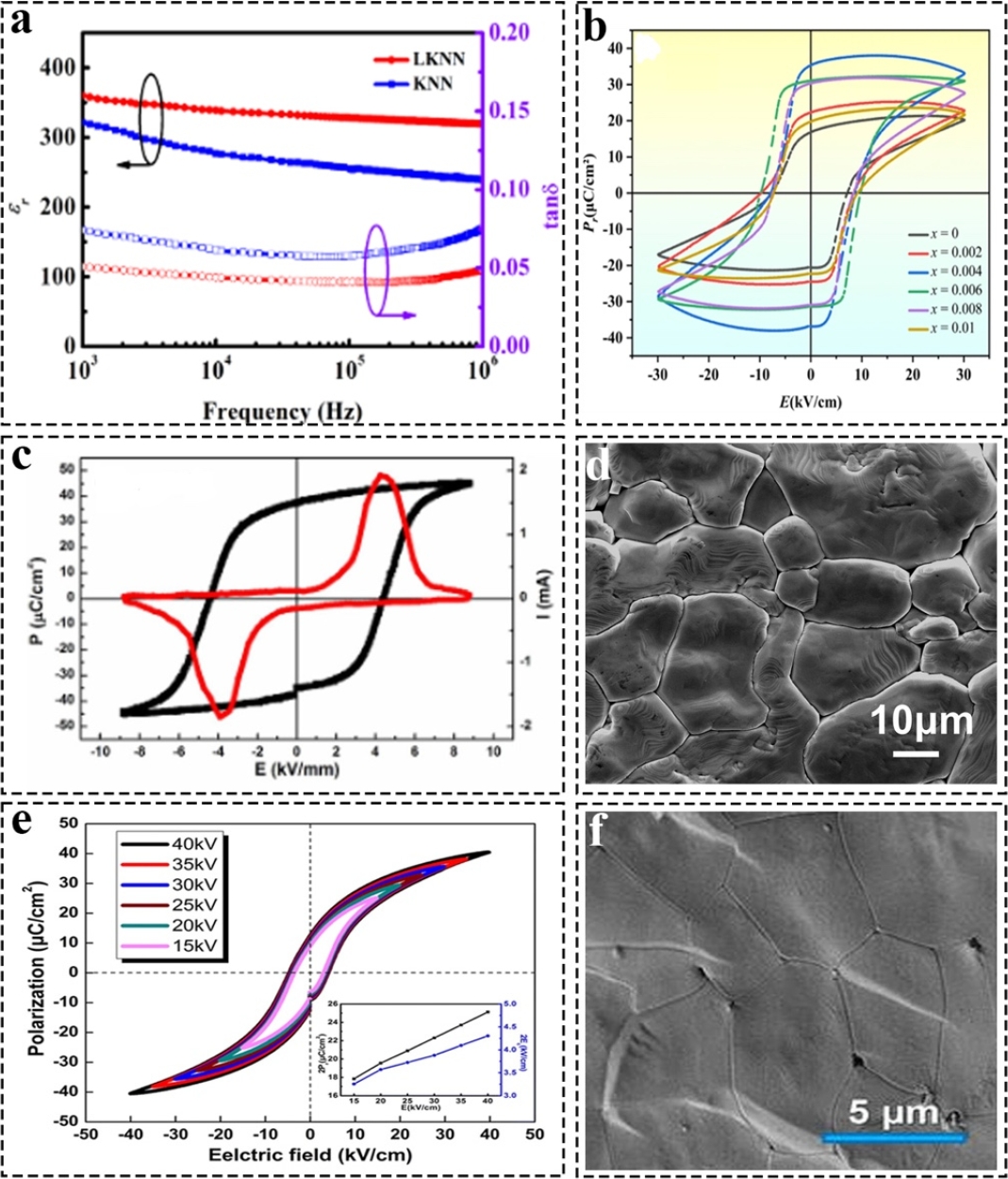
45] reported that the Li doped samples showed well-saturated P-E hysteresis loops compared to the pure KNN films. The LKNN film exhibited superior ferroelectric properties, with a high Pr of 9.3 μC/cm² and a Ps of 41.2 μC/cm² [
Figure 3(a)]. Besides, the substitution of the Li ions increased the piezoelectric properties of the film, resulting in a d
33 value of 105 pm/V. A study done by Zeng et al. [
46] reported large visible bulk KNN-based crystals with high compactness and low porosity, which were grown through the solid-state crystal growth method. Through appropriate Li addition, the growth, phase percentage, domain structure, and crystal quality were optimized, thereby enhancing the crystals' piezoelectric and ferroelectric properties as shown in
Figure 3(b).
2.1.3 Bismuth Sodium Titanate
Bismuth sodium titanate (Bi
0.5Na
0.5TiO
3, BNT) has evolved from a basic lead-free perovskite into the core of a very rich family of high-performance piezoelectric and electrostrictive ceramics through structural understanding, compositional design, and extensive doping and solid-solution strategies [
47,
48].BNT was first reported by Smolenskii and co-workers in 1960, as an ABO
3 distorted perovskite with Bi
3+/Na
+ on the A-site and Ti
4+ on the B-site, crystallizing in a rhombohedral structure at room temperature with a pseudocubic lattice parameter of about 3.98 Å and a rhombohedral angle of roughly 89.7°[
47]. Structurally, it can be viewed either as Bi/Na cations at the corners of a cubic cell with Ti at the body center and O on face centers, or as a three-dimensional network of corner-sharing TiO
6 octahedra with Bi/Na sitting in the cuboctahedral A-site cages; in reality, long-range cation ordering is absent, and the A-site is statistically occupied. BNT exhibits a sequence of phase transitions: a ferroelectric (FE) rhombohedral state at room temperature, an FE– antiferroelectric (AFE) transition around 200°C, a rhombohedral– tetragonal transition near 540°C, and a tetragonal–cubic transition around 320°C, leading to diffuse dielectric anomalies and electrostrictive behaviour characteristic of relaxor-like perovskites. Single crystals show relatively large spontaneous polarization (∼38 μC/cm
2) and high coercive fields (∼73 kV/cm), with piezoelectric coefficients d
33 on the order of 60–120 pC/N and strong orientation dependence. In contrast, polycrystalline ceramics typically exhibit lower macroscopic coefficients due to random domain orientation and grain-size effects [
49]. Because pure BNT alone could not match PZT-grade piezoelectric performance, a major development was forming solid solutions with bismuth potassium titanate, Bi
0.5K
0.5TiO
3 (BKT), which is tetragonal at room temperature but difficult to densify in single-phase ceramic form due to secondary phase formation during sintering [
50].
A major conceptual development has been the elucidation of the mechanisms underlying the giant electric-field-induced strain observed in BNT-based compositions, especially those modified with BTO, K
0.5Na
0.5NbO
3, BiAlO
3, and various dopants. One central mechanism is electric-field-induced phase transition: Near FE/AFE or FE/non-polar compositional boundaries, an applied field drives a reversible transition from a non-polar or weakly polar state to a long-range ferroelectric state. This transition involves significant changes in unit-cell volume or symmetry, producing large macroscopic strains. Upon field removal, the system relaxes back to the non-polar state, yielding large but largely recoverable strain loops [
51–
53]. Another mechanism involves domain switching, particularly point-defect-mediated reversible domain switching: aliovalent dopants create defect dipoles that align with spontaneous polarization and exert internal bias or restoring fields, enabling large but reversible domain reorientation under cyclic fields without complete depoling [
54]. BNT ceramics exhibit a high Curie temperature (≈320°C), large dielectric constant (εr), excellent thermal stability, and strong compatibility with silver electrodes, making them highly promising materials for use in dielectric ceramic capacitors [
55,
56]. Jia et al. [
57] study demonstrated a dielectric spectrum in which BNT ceramic exhibited diffusion phase transition behavior with two dielectric anomaly peaks, which is considered to be the reason for its good dielectric temperature stability. At low temperatures and high frequencies, BNT exhibits a relatively low dielectric loss (tan δ). Although its breakdown strength (E
b) is lower than that of other lead-free ceramics such as K
xNa
1−xNbO
3 or SrTiO
3, BNT demonstrates an exceptionally high maximum polarization (P
max ≈ 40 μC/cm²) and a quasi-double P–E hysteresis loop in the 200–320°C range, making it a strong candidate for energy storage applications. However, BNT also presents a large remanent polarization (Pr ≈ 38 μC/cm²) and a high coercive field (Ec ≈ 70 kV/cm). Additionally, a study by Xu et al. [
58] demonstrated that increasing the content of NaNbO
3 in BNT ceramics improved the dielectric temperature stability in lowtemperature regions while maintaining high permittivity. As a result, Bi³⁺ and Na⁺ ions were readily volatilized during sintering, leading to increased leakage conductivity and reduced breakdown strength [
Figure 3(c)]. A straightforward approach to improving BNT involves A-site modification by substituting Na⁺ or Bi³⁺ with alternative cations such as Rb⁺, Gd³⁺, Ho³⁺, K⁺, or Li⁺. This strategy helps refine the sintering behavior and tune the dielectric and ferroelectric characteristics of the material. Specifically, replacing A-site Na⁺ with Rb⁺ in BNT ceramics causes the grain morphology to become increasingly irregular with higher Rb⁺ content, while a 1 mol% Rb⁺ substitution lowers the E
c from 64.5 kV/cm to 59.7 kV/cm [
59]. Zannen et al. [
60] fabricated BNT–Gd ceramics, where the rare-earth ion Gd³⁺ diffused into the lattice and substituted for Bi³⁺. According to the authors, a pronounced reduction in the maximum dielectric constant (εm) due to A-site disorder was reported, along with a significant decrease in both Ec and remanent polarization (Pr). Moreover, a double P–E hysteresis loop appeared at 100°C, indicating an antiferroelectric-like behavior. Additionally, Xiao et al. [
61] employed K⁺/Li⁺ cosubstitution for Na⁺ in the composition Bi
0.5(Na
1-x-yK
xLiy)
0.5TiO
3, effectively reducing the Ec to a lower range of 2.47–5.16 kV/mm. Under this modification, ferroelectric P–E loops exhibiting relatively high remanent polarization (P
r ≈ 33.8–40.4 μC/cm²) were achieved around 200°C.
2.1.4 Barium Calcium Zirconium Titanate
Lead-free barium calcium zirconium titanate (Ba
1−xCa
xZr
yTi
1−yO
3, BCZT) ceramics have been synthesized via various routes to achieve phase-pure perovskite structures with optimized microstructures, thereby addressing the high-temperature requirements of conventional methods. The solid-state reaction remains prevalent, typically involving calcination at 1,200– 1,300°C and sintering at 1,400–1,540°C [
62–
65]. A study done by X. Ji et al. [
66] demonstrated a synthesized high-performance Ba
0.85Ca
0.15Ti
0.9Zr
0.1O
3 ceramics using the sol-gel method, sintering them at 1,400°C to achieve a uniform microstructure and impressive relative density of 5.56 g/cm³. This processing route ensured phase-pure perovskite formation, yielding excellent dielectric, ferroelectric, and piezoelectric properties that are competitive with those of lead-free PZT alternatives, as shown in
Figures 3(d) and
3(e). This work demonstrated strong permittivity for capacitor and energy-storage applications. Ferroelectric characterization revealed a Pr of 24.48 μC/cm², indicative of robust polarization switching and retention suitable for memory and actuator devices. Complementing these, the piezoelectric coefficient reached d
33 = 492 pC/N, positioning the material as a viable option for sensors and transducers. Further, X. Yan et al. [
67] advanced the sol-gel synthesis of nanocrystalline Ba
0.85Ca
0.15Ti
0.9Zr
0.10O
3 powders by optimizing sintering routes, dramatically improving densification kinetics and reducing the required sintering temperature from 1,540°C to 1,280°C while maintaining high electrical performance. Their conventional sintering conditions accelerated the sintering rate of nanocrystalline precursors, enabling fully dense ceramics with enhanced grain uniformity and phase purity at lower energy input compared to traditional high-temperature solid-state methods [
Figure 3(f)].
Additionally, Liu and Ren[
68] reported a lead-free (1-x) BaZr
0.2Ti
0.8O
3–xBa
0.7Ca
0.3TiO
3 (BZT-xBCT) system, establishing a morphotropic phase boundary (MPB) between rhombohedral (BZT-rich) and tetragonal (BCT-rich) phases that unlocked giant piezoelectric performance rivalling PZT. This composition exhibited a pivotal cubic-rhombohedral-tetragonal (C-R-T) triple point at x ≈ 0.32 and ~57°C, enabling enhanced polarization rotation and electromechanical coupling. Their ceramics achieved extraordinary ferroelectric metrics, including the highest spontaneous polarization P
s ≈ 20 μC/cm², remnant polarization P
r ≈ 15 μC/cm², lowest Ec ≈ 0.168 kV/mm, and relative permittivity εr ≈ 3,060.W. Li et al. [
69] fabricated Ba
0.92Ca
0.08Ti
0.95Zr
0.05O
3 thin films via solgel on Pt/Ti/SiO
2/Si and LNO/Pt/Ti/SiO
2/Si substrates, achieving dielectric constants of 550 and 620 at 100 kHz, respectively, with temperature-dependent peaks near 75°C. The LNO-buffered films exhibited 64% tunability under applied fields, attributed to enhanced lattice matching and epitaxial growth, which promote higher permittivity and field responsiveness. Besides, Y. Zhang et al. [
70] synthesized pure and Mn-modified Ba
0.95Ca
0.05Zr
0.1Ti
0.9O
3 ceramics using the solid-state method, investigating Mn doping (0-2 mol%) and sintering temperature effects on dielectric properties. Optimal 1.2 mol% Mn doping yielded εr = 1,651 (vs. 1,314 undoped) and exceptionally low tan δ = 0.0294% at room temperature, with sintering at 1,450°C promoting dense microstructure and reduced oxygen vacancies for “hardening” behavior.
2.1.5 Barium Calcium Tin Titanate
Barium calcium tin titanate (Ba
0.98Ca
0.02Sn
0.04Ti
0.96O
3, BCST) stands as a promising lead-free piezoceramic material derived from BTO through targeted substitutions of Ca²⁺ at the A-site and Sn⁴⁺ at the B-site. This composition adopts the classic ABO₃ perovskite structure, most often crystallizing in a tetragonal phase with P4mm symmetry or coexisting orthorhombic and tetragonal phases, depending on the synthesis conditions. The incorporation of Ca (x=0.12) effectively lowers the orthorhombic-to-tetragonal (T
O-T) and rhombohedral-to-orthorhombic (T
ro) phase transition temperatures, while Sn (y=0.06) depresses the Curie temperature to around 70-78°C yet strategically positions polymorphic phase transitions (PPT) near room temperature. Such engineering creates lowenergy barriers for polarization rotation, closely mimicking the superior electromechanical response of PZT at its morphotropic phase boundary, all without lead's environmental toxicity. As a lead-free alternative, BCST addresses the RoHS-driven phase-out of PZT, which has long dominated piezoelectrics with d₃₃ values exceeding 500 pC/N but also poses health and ecological risks. Through optimized processing, such as solid-state synthesis followed by sintering at 1,300-1,450°C or high-energy ball milling to produce 7-10 nm nano powders, BCST achieves competitive metrics [
71–
75].
Naveen et al. [
72] synthesized lead-free BCST via solid-state reaction. Calcination above 1,150°C yielded pure tetragonal P4mm perovskite (a=4.00 Å, c=4.02 Å), with pellets sintered at 1,200–1,300°C. FE-SEM revealed grain growth from 12.8 μm (1,200°C) to 24.8 μm (1,300°C). Optimized 1,300°C sintering delivered εᵣ=6,100 (1 kHz, Tc=70°C), Pᵣ=3.38 μC/cm², and d₃₃=236 pC/N superior to lower temperatures due to enhanced domain mobility and reduced porosity. Chitra et al.[
75] studied the low Curie temperature of BCST via high-energy ball milling (HEBM). Precursors (BaCO₃ 99%, TiO₂ 99.5%, SnO₂ 99%, CaCO₃ 99.5%) were conventionally milled, calcined (1,150°C, 4 h), then planetary-milled (175 rpm, 5 h each), pressed (320 MPa), and sintered (1,375°C, 4h) into BCST100-BCST400 samples. According to the XRD analysis, a pure-phase perovskite (tetragonal P4mm • orthorhombic Amm
2) was confirmed, with a crystallite size of ~41 nm. SEM revealed grains up to 13.54 μm, with a density peaking at 5.495 g/cm³. According to the hysteresis loop analysis, the material had Pᵣ = 4.92 μC/cm², Ec = 2.19 kV/cm, and d₃₃ = 240 pC/N post-poling. Besides, Baraskar et al. [
71] conducted a comprehensive structural analysis on (1-x) BCZT-xBCST ceramics, revealing phase-pure perovskite formation across x=0-1.0 via XRD, where the (002)/(200) doublet near 45° 2θ transitioned from orthorhombic-dominant at x=0 to tetragonal-dominant at x=1.0, reflecting Zr⁴⁺→Sn⁴⁺ substitution effects on ionic radii (0.72 Å→0.69 Å). Rietveld refinement using dual-phase models (ICSD-186460 Amm
2 orthorhombic + ICSD-245946 P4mm tetragonal) provided excellent fits (Rwp=6.8-8.5%, χ²≈1.6-2.4): orthorhombic content decreased from 69% (x=0) to 39% (x=1), while tetragonal increased from 31% to 61%, with lattice parameters of ~a=4.00 Å, b=5.66 Å, c=5.68 Å (V≈129 ų) for orthorhombic and a≈4.01 Å, c≈4.04 Å (c/a=1.006-1.008, V≈65 ų) for tetragonal phases. Complementary techniques validated this analysis, where the Raman spectroscopy tracked phonon modes (3LO/3TO→1LO/1TO), confirming rhombohedral→ orthorhombic →tetragonal → cubic transitions with TO-T shifting from 28°C (x=0) to 6°C (x=1) near room temperature. This analysis demonstrated Sn⁴⁺ substitution stabilizing the tetragonal phase while maintaining orthorhombictetragonal coexistence at room temperature, providing 18 polarization vectors and low-energy rotation barriers that explain the peak d
33=360 pC/N performance at x=0.4.
2.1.6 Aluminum Nitride
Aluminum nitride (AlN) ceramics have undergone substantial development across growth mechanisms, sputtering process optimization, doped systems, and application-oriented engineering, with magnetron sputtering emerging as the central, industrially relevant route for high-quality piezoelectric and thermally conductive films [
76,
77]. AlN crystallizes in the hexagonal wurtzite structure and typically grows with either 002 (c-axis) or 100/101 orientations, depending on the energy of arriving species and mean free path during deposition. Chirumamilla et al. [
78] pioneered seed-mediated control of AlN nanostructures via reactive magnetron sputtering on Si (111)/TiN substrates. Using ebeam-deposited Ag, Au, or Al nanoparticles (~100 nm) as seeds, they tuned nucleation to yield bud/flower-like pillars or lamellae with wurtzite crystallinity. Ag seeds produced the longest, tilted (33° at 85° glancing angle, GLAD) nanostructures via enhanced adatom mobility and shadowing, outperforming Au/Al in length and rate. Normal incidence yielded compact bud-shaped structures; GLAD formed open, high-roughness arrays with the c-axis along the columns, as confirmed by SEM/STEM-EDS (no interdiffusion), XRD, AFM, and PFM, which showed a giant piezoelectric response for energy harvesting. This scalable approach enables morphology-tailored AlN matrices for piezo-generators, sensors, and MEMS.
Additionally, a study by Sandager et al. [
79] advanced DC reactive magnetron sputtering of AlN thin films on Si (111) wafers by systematically mapping processing pressure (0.1–1.0 Pa), magnetron power (300–1,200 W), and N₂/Ar ratio (27–50%). All ~400 nm films showed wurtzite c-axis (002) orientation with tensile stress; optimal quality (FWHM 0.14°, RMS roughness 0.9 nm, dense columns) emerged at low pressure (0.2 Pa), high N₂/Ar (50%), and moderate power, balancing crystallinity against target poisoning and rate (up to 28.9 nm/min at 900 W, 27% N₂/Ar). Higher pressure induced Zone 1 tapered voids and defects via shadowing/scattering; power boosted the rate/energy for diffusion but raised stress; high N₂/Ar-densified films were akin to Zone 2. Their tendency diagram guides industrial trade-offs for piezo/HEMT buffers at low T (200°C). Ababneh et al. 80 study demonstrated that power (250–1,000 W), pressure (0.5–5 mTorr), N₂/Ar ratio (10–50%), and substrate bias critically tune texture, with high power/low pressure favoring columnar growth and piezo-response (d₃₃ ~5 pm/V). Their work benchmarks sputtering for scalable resonators and compares orientations: c-axis yields d₃₃=3 pm/V, d₃₁=-1 pm/V vs. weaker (101). Wei et al. [
81] demonstrated target-substrate distance (TSD) as the dominant driver of AlN orientation on Si (100) wafers via RF-MS. Short TSD/high-energy particles yield dense columnar (002) “raspberrylike” grains; longer TSD/low-energy particles favor non-columnar (100) “rose-like”; intermediates mix both with reduced thickness via energy minimization. Pressure/temp refined shifts, linking kinetics/bonds to piezo-tailored MEMS.
Organic piezoelectric materials represent a class of polymers and bio-derived compounds that exhibit piezoelectricity through noncentrosymmetric molecular arrangements, enabling the direct conversion of mechanical stress into electrical charge. These materials, typified by polyvinylidene difluoride (PVDF) and its copolymers, display semi-crystalline structures where electroactive phases (e.g., PVDF's β-phase) align dipoles for enhanced piezoelectric coefficients, typically 20–35 pC/N in d
33 mode, lower than ceramics but adequate for flexible applications [
82]. Key examples include odd-nylons, polyimides, and biopolymers like poly-L-lactic acid (PLLA) or collagen, offering low acoustic impedance and biocompatibility. Unlike rigid inorganic piezoelectrics (e.g., PZT), organic variants provide superior flexibility, lightweight design, and solution processability for scalable fabrication via electrospinning or 3D printing, ideal for wearables, sensors, and implants. Phase engineering through stretching, poling, or nanofillers amplifies performance, bridging the gap with inorganics for energy harvesting [
5,
83].
2.2.1 Polyvinylidene Difluoride
Polyvinylidene difluoride (PVDF), exhibits a piezoelectric coefficient of 24-34 pC/N in its poled β-phase, achieved through stretching and poling to align dipoles. PVDF β-phase advancements focus on transforming the nonpolar α-phase into the electroactive β-phase, which aligns dipoles to achieve superior piezoelectricity [
82,
84,
85]. PVDF naturally favors the non-polar α-phase (50-60% crystallinity), but the all-trans β-phase maximizes dipole moments via stretching, poling, annealing, or additives that nucleate β-crystals. Techniques like solvent casting with acetone boost β-content by slowing evaporation and aligning chains; higher PVDF concentration or electric fields further enhance it beyond 50%. Electrospinning, UV/plasma treatments, or rolling after hotpressing yield sharp β-peaks at 840 cm⁻¹ (FTIR) [
86]. Therefore, over the years, researchers have worked closely to enhance the piezoelectric properties of this material by increasing its β-phase content. A study done by Liu et al. [
84] demonstrated that ionic liquid-assisted 3D printing achieved 98.3% β-phase without poling, delivering 4.7x voltage and 17.5 nA/cm² current via fused deposition modeling. They applied flash annealing, which transformed α/γ to β in PVDF-TrFE fibers, boosting modulus/tensile strength while retaining flexibility; in-situ Raman/XRD confirms conformational switching, not new crystal growth. Thus, the biaxial stretching in PVDF/PMMA blends increased β-fraction and crystallinity for the films.
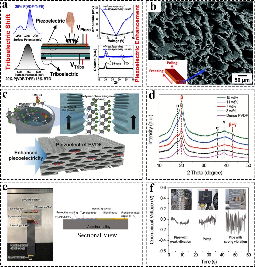
Recently, Jang et al. [
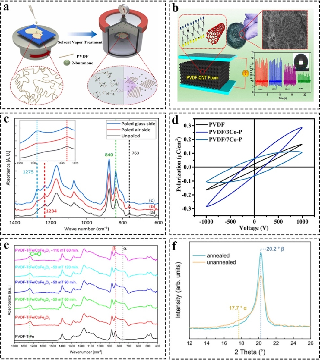
87] used solvent vapor annealing (SVA) for PVDF composites [
Figure 4(a)], yielding defect-free, high β-phase crystallinity that dramatically boosted the piezoelectric response, with superior voltage and current outputs compared with untreated films, enabling dual-controlled (strain/temperature) energy harvesters. Simadri et al. [
88] developed an ultralight PVDF foam using table salt as a sacrificial template and CNTs as reinforcement to achieve β-phase formation and nanostructured pores without applying electrical poling [
Figure 4(b)]. By utilizing the intrinsic hydrophobicity of PVDF, the high surface-to-volume ratio, and the conductive properties of CNTs, an innovative, high-performance, moisture-resistant, piezoelectric ultralight PVDF–CNT foam– based nanogenerator was developed for generating electric output even under humid conditions. Additionally, Morali et al. [
89] investigated the transformation from the γ- to β-phase in polyvinylidene fluoride (PVDF) nanocomposite films fabricated by solvent-evaporation-assisted 3D printing using BTO nanoparticles. While PVDF’s β-phase is responsible for its piezoelectricity, γ-phase formation often dominates in solution-based methods. They emphasized the role of annealing in enabling effective poling and analyzed the α-, β-, and γ-phases using FTIR, XRD, and DSC. After annealing, the PVDF-BTO films contained 76% β + γ phases (mainly γ), which increased to 93% after poling, with a 40% absolute β-phase fraction. The β-phase distribution, identified by the 1,275 cm⁻¹ FTIR peak [
Figure 4(c)], was found to be nonuniform and dependent on the poling field direction. These findings provide practical insights to enhance the piezoelectric performance of PVDF-based nanocomposites for sensing applications.
Furthermore, a study by Bahloul et al. [
90] achieved a breakthrough in high-β-phase PVDF composite thin films filled with metal phosphate particles (NiP, AgP, CoP, CoPn) synthesized via tailored hydrothermal, precipitation, co-precipitation, and solvothermal methods. The composites demonstrated exceptional β-phase content up to 96% at low 3-7 wt% loadings, unprecedented mechanical enhancements (181.83% tensile strength increase and 184.76% Young's modulus improvement in PVDF/3CoPn), and superior thermal stability (24.92°C higher onset degradation in PVDF/7NiP). Ferroelectric performance advanced markedly, with 200% higher remnant polarization (PVDF/7CoP) and 75% higher maximum polarization (PVDF/3CoP) [
Figure 4(d)], establishing critical structure-property correlations for lead-free, flexible energy-harvesting materials.
2.2.2 Poly(vinylidene fluoride-co-trifluoroethylene)
Poly(vinylidene fluoride-co-trifluoroethylene) (PVDF-TrFE) copolymer represents a significant advancement in organic piezoelectric materials, distinguished by its ability to spontaneously form the electroactive β-phase without the mechanical stretching or electrical poling typically required for pure PVDF. This unique property arises from the incorporation of trifluoroethylene (TrFE) monomer units, which introduce structural defects that lower the energy barrier for the all-trans β-conformation, thereby promoting higher crystallinity (often >60%) and enhanced dipole alignment during standard processing such as solution casting or melt extrusion [
4].
Several notable developments have been undertaken to underscore the PVDF TrFE’s versatility. A study by Fortunato et al. [
91] achieved a significant advancement in piezoelectric PVDF-TrFE nanocomposites by incorporating 5 wt% CoFe₂O₄ nanoparticles and applying low-intensity DC magnetic poling (50 mT at 65°C for 90 min), yielding a piezoelectric coefficient d₃₃ up to 39 pm/V comparable to or exceeding that of electrically poled PVDF-TrFE without requiring high-voltage electrodes or fields. This poling method aligns β-phase domains via nanoparticle-polymer interfacial stress and chemical bonding (as evidenced by new carbonyl FTIR peaks), rather than increasing β-phase content (which remains stable at ~82%), while mitigating aggregation at optimal fields as illustrated in
Figure 4(e). The approach offers a simple, cost-effective alternative for flexible energy harvesters and wearable sensors. Further, Hu et al. [
92] pioneered flash annealing (60 s at 130°C, above Curie temperature) for wet-processed PVDF-TrFE films, achieving record piezoelectric coefficients d₃₃ of 70.89 pm/V (PFM) or 68 pC/N (quasi-static) over twice commercial PVDF and superior to long-time annealed films via rapid β-phase crystal proliferation and preserved dipole orientation without chain relaxation [
Figure 4(f)]. In situ XRD, Raman, and MD simulations revealed reversible α-to-β phase transitions that drive increased β-crystallinity (highest Curie enthalpy) in electrospun/spin-coated films, unlike in melt-processed films. The treated films excelled in energy harvesting (7.53 μW/m²), highfrequency sensing (down to 124 mN at 200 Hz), and health monitoring (cough/swallow detection), enabling scalable, lowenergy production of high-performance, flexible piezoelectronics. Besides, Chauhan et al. [
93] demonstrated an optimized spincoating parameter (15 wt% PVDF-TrFE in DMSO, 130°C annealing) to grow highly crystalline β-phase PVDF-TrFE thin films on low-cost, flexible Mo/PET substrates, enabling fabrication of a cantilever-based piezoelectric energy harvester (PEH) with 48 Hz resonance. The device delivered a peak power of 6.83 μW at 1 g acceleration across 2.24 MΩ (power density 312.85 μW/cm³), outperforming similar flexible PVDF-TrFE PEHs on PDMS or CNT substrates due to uniform film morphology and maximized strain near the fixed end. A novel mass-spring-damper model incorporating mechanical (Cd=0.035) and electrical damping accurately predicted voltage/power outputs, validating the design for low-frequency wireless sensors in agriculture/water monitoring. Additionally, Beigh et al.[
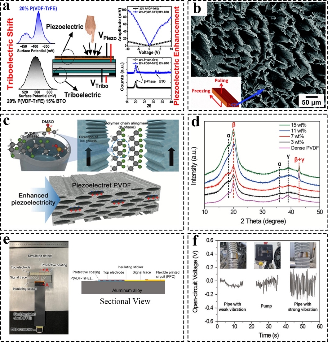
94] optimized BTO nanoparticle doping in PVDF-TrFE (15 wt% BTO in 20 wt% PVDF-TrFE solution, 130°C annealing), achieving maximal β-phase crystallinity (81%) and a piezoelectric coefficient d₃₁ of 0.58 nm/V, 9 times higher than pristine PVDF-TrFE via enhanced dipole alignment and hydrogen bonding at BTOpolymer interfaces [see
Figure 5(a)]. KPFM revealed a triboelectric shift from negative (–382.5 mV) to positive (495 mV) surface potential with superior charge retention (V₂₀₀ drop to 60 mV), enabling dual-mode transduction in a flip-chip hybrid sensor (sensitivity 21 mV/kPa triboelectric, 9.2 mV/kPa piezoelectric; 1– 60 kPa range, <7.2% hysteresis). The low-crosstalk design distinguished press/tap/rub gestures, advancing self-powered biomechanical sensing for wearables and tactile interfaces.
2.2.3 Ferroelectrets
Ferroelectrets, particularly charged cellular polypropylene (PP) foams, are lightweight, compressible polymer films with lens or plate-like voids that trap charges during high-field poling, functioning as deformable macro-dipoles to produce quasipiezoelectric responses with d
33 coefficients exceeding 100–300 pC/N, far surpassing molecular-dipole polymers like PVDF while maintaining Young's moduli below 10 MPa [
95]. Miao et al. [
96] pioneered nanoscale characterization of cellular polypropylene (PP) electret films using piezo response force microscopy (PFM), revealing localized d₃₃ of 7–11 pC/N via dual-frequency resonancetracking PFM, confirming inhomogeneous piezoelectricity from void deformation. SS-PFM demonstrated ferroelectric-like asymmetric phase hysteresis and amplitude butterfly loops from charge-state switching via barrier discharges, validated by SSPFM-waveform D-E loops (switchable polarization ~0.3 μC/cm² at 175 kV/mm, non-saturating vs. PVDF's 1.8 μC/cm²). These findings distinguish electret pseudo-ferroelectricity from true ferroelectrics, guiding reliable assessment of microscopic versus macroscopic properties for high-d₃₃ polymer applications.
Martynas et al. [
97] study demonstrated a breakthrough in ferroelectret technology by engineering cellular polypropylene (PP) foam films starting twice as thick (90 μm vs. conventional 34–70 μm). Through optimized gas-diffusion expansion and thermal treatment, they expanded films to 321 μm thickness (densities down to 179 kg/m³), yielding mechanically ultra-soft structures (minimum elastic stiffness c33 = 0.97 MPa) and high piezoelectric coefficients (d
33 up to 130 pC/N at 10 kV charging, onset threshold 3.5 kV). This simultaneously lowered the thickness-extension resonance frequency to 233 kHz, an order of magnitude below prior high-kHz/MHz values, eliminating the need for complex multilayer stacking in low-frequency airborne ultrasonic transducers. Recently, Li et al. [
98] demonstrated a transformative class of cellular polymer electrets, predominantly polypropylene (PP) and fluorinated ethylene propylene (FEP), exhibiting ultrahigh piezoelectric coefficients (d
33 up to 6,500 pC/N) and acoustic impedance closely matched to air (~0.03 MRayl). These attributes stem from dielectric barrier discharges during high-field corona poling (5–10 kV/mm), which trap bipolar charges on void surfaces, enabling elastic dipole deformation under biomechanical stress. Zhang et al. [
99] pioneered the application of ice-templating (freeze-casting) to fabricate porous PVDF ferroelectrets with unidirectionally aligned, elongated pore channels (20–25 μm diameter, 24–78% porosity) via DMSO solutions (2–12 wt% PVDF), marking a cost-effective, environmentally benign alternative to mechanical stretching or chemical templating [
Figure 5(b)]. This foundational development demonstrated high piezoelectric d
33 coefficients (peak 264 pC/N in 78% porosity samples), rivaling those of commercial PP ferroelectrets, achieved via Townsend breakdown during corona poling (26.8 kV), with low permittivity (εr ≈ 1.5–3.5) yielding superior figures of merit (g33 ≈ 20 V m/N, comparable to PZT). Aging stabilization and γ-phase dominance further underscore the viability of ferroelectrets for flexible sensors and vibration harvesting.
Jeon et al. [
100] introduced a ground-breaking eco-friendly gradient ice-templating method to fabricate unidirectionally porous PVDF piezoelectrets, achieving an electroactive β-phase fraction of 86.77% (versus 72.63% in dense PVDF) through controlled PVDF concentrations (3–15 wt%) in DMSO solvent. This yielded hierarchically porous structures with vertically aligned pores (51–144 μm in diameter, 59.6–92% porosity) and a longitudinal piezoelectric coefficient d
33 of 29 pC/N, which is higher than that of dense PVDF [
Figures 5(c) and
5(d)]. The seminal development demonstrated that these piezoelectrets generated peak outputs of 35 V and 1.1 μA (3.56 μW/cm²) under 10 N compression, validated by Multiphysics simulations that confirmed pore-induced strain concentration and dipole amplification. Remarkably, the devices exhibited dual functionality, harvesting energy from falling water droplets while reducing organic contaminants in seawater/rainwater (UV-Vis confirmed), establishing gradient ice-templated PVDF piezoelectrets as a self-powered platform for sustainable environmental IoT monitoring and portable water purification.
Further studies were done by Cha et al. [
101] who introduced a template-assisted strategy for fabricating porous PVDF-based piezoelectric nanogenerators, positioning nanoporous architectures as a robust alternative to conventional one-dimensional nanowire generators. In their approach, vertically aligned ZnO nanowires or Si pillar arrays serve as removable templates; PVDF solution is infiltrated, thermally converted to the electroactive phase, and the template is selectively etched, yielding vertically penetrating nanopores with sub-micrometer interpore spacings and film thickness on the order of a few micrometers. This lithography-free route circumvents the material limitations of nanowire growth, enabling the integration of high-efficiency polymeric piezomaterials, such as PVDF, into nanostructured energy harvesters. The key advance lies in exploiting geometric strain confinement within closely spaced nanopores to amplify piezoelectric response. Finiteelement electromechanical modeling shows that reducing interpore distance increases effective d
33 and local piezoelectric potential along the poling direction, as lateral strain relaxation is suppressed and the effective coefficient approaches the intrinsic d
33 of PVDF. Experimentally, sonic-wave-driven porous PVDF nanogenerators exhibit open-circuit voltages and short-circuit currents several times higher than those of bulk-film PVDF devices under identical acoustic excitation, yielding rectified power densities on the order of tenths of milliwatts per cubic centimeter. The devices can charge capacitors to voltages sufficient to drive commercial LEDs using only sound as the input, demonstrating continuous low-level power generation from weak mechanical stimuli.
3 Application of Flexible Piezoelectric Materials
Piezoelectric materials can harvest energy directly from structural vibrations and ambient mechanical waste sources in infrastructure systems (such as bridges and buildings), as well as in biomedical, healthcare, and medical devices. In addition to energy harvesting, these materials play a crucial role in the fabrication of transducers, actuators, and surface acoustic wave (SAW) devices. In this section, we present a categorized overview of existing piezoelectric applications related to vibrational energy sources, mechanical waste energy recovery, fluid-dynamic harvesting systems, and biological or biomedical energy harvesting approaches [
102].
Piezoelectric sensors use the direct piezoelectric effect to turn mechanical stimuli, such as stress, strain, pressure, vibration, or acoustic waves, into measurable electrical signals. They offer high sensitivity, wide bandwidth, and low power consumption, making them perfect for real-time structural health monitoring (SHM). These sensors come in various setups, including charge-mode and integrated electronics piezoelectric (IEPE) accelerometers for detecting vibration and shock in aerospace, automotive, and industrial machinery; pressure and force transducers for process control and fluid dynamics; and surface acoustic wave (SAW) or quartz crystal microbalance (QCM) devices for accurate mass, gas, chemical, and biosensing through frequency shifts caused by surface changes. In SHM, piezoelectric transducers, especially piezoelectric wafer active sensors (PWAS), enable both active and passive damage detection by serving as co-located actuators and sensors. A key method involves propagating ultrasonic Lamb waves in plates and thin structures, where PWAS actuators generate multimodal guided waves (e.g., A0, S0 modes) that travel long distances with little attenuation and are highly sensitive to defects such as cracks, delaminations, corrosion, or impacts[
103]. A review by Min Ju et al[
104] delineated piezoelectric sensing applications in structural health monitoring (SHM) across active and passive modalities. Electromechanical impedance (EMI) techniques enable local detection of cracks, debonding, corrosion, and joint looseness in concrete, composites, rotary blades, and bolted joints. Guided-wave/ultrasonic propagation enables global damage assessment in aircraft, pipelines, pressure vessels, bridges, and bonded joints using pitch-catch, pulse-echo, and thickness modes. Passive acoustic emission monitors impact, crack propagation, delamination, and fatigue in metallic plates and composites, while stress monitoring evaluates dynamic loads in bridges and wings. Hybrid systems integrate these to provide a comprehensive evaluation of pressure vessels, sailplanes, and concrete structures. Wong et al. [
105] demonstrated the applications of active ultrasonic sensing for structural health monitoring (SHM), leveraging Lamb wave (S₂ mode at 3.2 MHz) propagation facilitated by in-situ fabricated direct-write transducer (DWT) arrays from PVDF-TrFE coatings [
Figure 5(e)]. These lightweight, conformal DWTs enable pulse-echo imaging of defects on metallic plates (e.g., aluminum alloy with simulated 45 mm × 2 mm × 1 mm notches), pipes, carbon fiber-reinforced polymer plates, and fastener holes, supporting detection of fine cracks (<1 mm), corrosion progression, thickness loss, and adhesive joint integrity via sequential ultrasonic scans and edgecomputing signal processing (FIR filtering, envelope detection, decimation by 40×). Broader implementations encompass buildings, bridges, railway tracks, aircraft, and maritime structures, where DWT networks reduce data transmission by 331× and energy by 224× through on-node processing before ZigBee wireless relay to IoT/cloud platforms, enhancing scalability for real-time, wide-area integrity assessment under fatigue and corrosion. A recent study by Dattar et al. [
106] showed applications of reusable magnet-bonded piezoelectric sensors (MBPS) for electro-mechanical impedance (EMI) and vibrationbased SHM in steel structures, targeting bolt looseness, cracks, stiffness loss, and holes via RMSD (RDI), curvature (CDI), and fused hybrid damage index (HDI). MBPS configurations demonstrated a high repeatability (>99.5% CC) and sensitivity proportional to sensor-magnet size ratio on miniature plates (250×200×3 mm) and large thin-walled plates (1,200×970 mm), detecting multi-state damage (central/edge holes) with peak indices at damage sites amid adjacent noise. Global modal analysis extracts strain mode shapes (first five modes) for CDI, while EMI (100–500 kHz) yields local RDI; HDI (multiplicative square fusion) suppresses undamaged noise, enhancing localization for scalable, non-bonded monitoring in infrastructure like bridges and buildings
Piezoelectric actuators exploit the converse piezoelectric effect to transform electrical input into precisely controlled mechanical displacement, force, or deformation, which has made them central to high-resolution positioning systems, adaptive structures, and micro-mechanical devices. In their most common form, multilayer stack actuators consist of many thin piezoceramic layers (often PZT) with internal electrodes connected in parallel, allowing large strain under relatively low voltages and generating blocking forces in the kN range while maintaining micrometer- or sub-micrometer-scale stroke. These stacks are integrated into flexure-guided mechanisms, such as lever or bridge amplifiers, that convert small axial strains into larger output displacements with well-defined motion trajectories and virtually zero backlash, enabling fast, repeatable actuation in nanopositioning stages, scanning systems, and precision dispensers. Bimorph and unimorph bending actuators, comprising asymmetric piezoelectric layers bonded to elastic substrates, generate relatively large tip deflections with modest voltages and are widely used in microvalves, adaptive optics, relay devices, and microrobotic manipulators, where compactness and low power consumption are critical [
107].
A study by Guo-Ying Gu et al. [
108] demonstrated impressive results from an integrated control strategy applied to a piezoceramic stack actuator (PSt 150/100/VS12) within a onedimensional monolithic flexure-based nanopositioning stage, driven by voltages up to 150 V and measured using an integrated strain gauge sensor. This approach effectively compensates for hysteresis, creep, and vibration, enabling high-precision motion control. The complete controller combining hysteresis feedforward, the notch filter, and a high-gain PI feedback loop boosted closedloop bandwidth dramatically from 65-67 Hz to 605 Hz. It achieved RMS tracking errors below 1% across frequencies (e.g., 0.93% at 100 Hz sinusoids), step responses settling within 2 ms to a 5% error band, and elimination of steady-state creep errors, confirming superior speed and accuracy. Further study by Shiuh et al. [
109] applied surface-bonded PZT patches to cantilever beams and clamped plates, achieving 25-40% vibration amplitude reduction at first resonant modes (∼50-200 Hz) using positive position feedback (PPF) control and optimal patch placement via modal strain energy methods. Finite element simulations and experimental modal analysis under harmonic base excitations confirmed mode shape tailoring, with spill-over effects minimized below 10% via collocated sensor-actuator pairs. Similarly, composite laminate plates showed suppressed vibrations via PZTinduced strains, reducing peak displacements by up to 35% in multi-mode scenarios.
Piezoelectric energy harvesting (PEH) enables autonomous power supply for low-energy electronics by converting ambient mechanical vibrations, motion, and fluid flows into electrical energy. Common architectures encompass resonant cantilever designs (unimorph or bimorph with tip masses), frequency-tuned for prevalent vibrations in machinery, bridges, and human activity; non-resonant broadband or nonlinear configurations employing mechanical stoppers, bistable mechanisms, or multi-degree-offreedom systems to broaden operational frequency ranges; flowinduced vibration harvesters leveraging vortex-induced vibration, flutter, or galloping in air/liquid flows for applications like pipeline and environmental sensing; and nanogenerator arrays utilizing ZnO nanorods, PZT nanofibers, or PVDF nanowires with optimized zigzag or interdigitated electrodes to enhance strain capture efficiency [
2]. Recently, Cho et al. [
110] developed a roadcompatible PEG using piezoelectric transducers fixed at both ends, with the stress converging toward the centre of the device via a rigid bar. The device was tested in actual road conditions for 5 months, during which it was subjected to vehicles travelling at 10-50km/h as they entered a highway rest area. From the analysis, it was deduced that vehicles traveling at 50km/h generated 2.381W of output power, while those traveling at 10 km/h generated 576 mW. This generated energy powered the LED indicators and transmitted real-time information about the sensor’s leak, temperature, and strain.
Notably, Jeong et al. [
111]achieved a breakthrough in flexible piezoelectric energy harvesting by developing a scalable laser liftoff (LLO) process using XeCl excimer laser (420 mJ/cm²) to transfer 2 μm-thick PZT thin films from sapphire to PET substrates, preserving tetragonal crystallinity and piezoelectric response (d₃₃ ~50-60 pm V⁻¹). They fabricated high-density Au/Cr interdigitated electrodes (100 μm fingers, 50 μm gaps) with SU-8 passivation, enabling robust operation for 3,000 bending cycles while generating peak outputs of 140 V and 10 mA from finger flicking, sufficient to power a 3×3 flexible vertical LED array without rectification. This industry-compatible fabrication yielded an energy conversion efficiency of 11.8%, establishing a mechanically stable platform for self-powered bio-implantable optoelectronics. Additionally, a study done by Kim et al. [
112] pioneered flexoelectric-boosted piezoelectricity in lead-free BaTiO₃@SrTiO₃ (BT@ST) core-shell nanoparticles (NPs, ~400 nm) via facile hydrothermal synthesis (200°C, 6–18 h), forming a composition-graded SrTiO₃ shell (33.5–81.4 nm thick) that induces lattice strain gradients from ionic radius mismatch (Sr²⁺ 1.32 Å vs. Ba²⁺ 1.49 Å), enhancing effective d₃₃ by ~200% (49.6 pm V⁻¹ at 6 h shell) versus pure BT NPs. Multiscale simulations (DFT for phase stability, FEM for diffusion/strain) confirmed that an optimal thin-shell (6 h) maximizes flexoelectric coupling without paraelectric dominance. Flexible PDMS nanocomposites (20 wt% NPs, sandwiched in ITO-PET) yielded record d₃₃ (118 pC/N), output voltage (~160 V), and current (~700 nA) under 0.3% strain, outperforming prior lead-free NPs/composites for energy harvesting.
Recently, Jang and co-workers [
113] created a simple 15 μm-thick flexible piezoelectric energy harvester by sandwiching a conductive PEDOT: PSS layer between two PVDF polymer layers using spin-coating and drop-casting on a plastic substrate. The conductive interlayer boosted β-phase PVDF crystallinity to 85% through electrical poling that permanently aligns dipoles across interfaces, delivering 4× higher output (2.28 V, 0.58 μA vs. 0.61 V, 0.125 μA for plain PVDF) from finger bending. Unlike regular PVDF devices that degrade after one month, this all-polymer design showed no performance drop after 15,000 cycles and 6 months, enabling reliable vibration sensing on curved pipes matching commercial PVDF sensors [
Figure 5(f)].
Piezoelectric transducers are central in medical ultrasound imaging, minimally invasive therapies, and emerging self-powered wearables and implants. Conventional bulk PZT transducers dominate diagnostic and therapeutic ultrasound and high-intensity focused ultrasound. Flexible piezoelectric materials and composites, for instance, PVDF-based polymers, electrospun nanofibers, and ceramic polymer composites have been intensively used in the fabrication of wearable and conformable systems [
9,
114].
A study done by Wang et al. [
115] made a flexible sensor by electrospinning P(VDF-TrFE) polymer with carbon nanotubes, then stretching it to properly align the polymer chains for maximum piezoelectric β-phase. The sensor showed good performance: 50 pm/V piezoelectric response, 0.986 GPa stiffness, and 540 mV per Newton sensitivity. Tests showed it could detect pulse, breathing muscles, and joint movements, making it promising for wearable health monitoring and disease diagnosis. Yu et al. [
116] made a flexible sensor by mixing BaTi0.88Sn0.12O
3 ceramic with glass fibers in PVDF polymer. The device detected very light touches (1–9 N force) with high sensitivity: 1.23 V N⁻¹ and 41 nA/N. It sensed human movements and even raindrops. During testing, it remained reliable after 5,000 cycles of 40 N pressure. Smart clothing still requires improvements in comfort and washability, but adhering soft sensors to the skin remains the primary research direction. To address the growing demand for wearable electronics, Guo et al. [
117] developed a wireless piezoelectric pressure sensor utilizing an electrospun PVDF/BTO nanowire fibrous membrane integrated with a wireless circuit incorporating data conversion control and Bluetooth modules. The device demonstrated high sensitivity to human motion patterns, including crouching, walking, and running, highlighting the potential of wireless piezoelectric sensors for applications in rehabilitation and sports medicine. Ma et al. [
118] developed a miniaturized, wearable self-powered piezoelectric textile sensor for biosensing applications. Compared to conventional equipment, this sensor offers high detection accuracy and real-time monitoring capability by capturing subtle muscle movements. The piezoelectric composite, comprising ZnO nanowires embedded in a PVDF matrix, generates electrical signals that correlate with motion speed, frequency, and joint angle. Specifically, as the joint angle increased from 44° to 84°, the output voltage decreased from 0.178 V to 0.049 V, demonstrating a clear relationship between bending degree and piezoelectric response. Additionally, Zhao et al. [
119] fabricated a flexible PVDF-based piezoelectric sensor and applied it to monitor basketball movements. Sensors attached to finger, elbow, and knee joints captured force magnitude, angular displacement, and motion frequency through PVDF's piezoelectric response. Shooting, jumping, and running actions were successfully converted into quantifiable electrical signals, demonstrating the potential of such sensors to enable big data collection in sports and advance Internet of Things (IoT) applications in athletic performance analysis.
Panahi et al. [
120] developed a cost-effective, low-frequency triangular piezoelectric sensor comprising a vertex-attached triangular beam constructed from PVDF and PDMS for continuous respiratory monitoring. The triangular geometry maximized voltage output through optimized strain distribution along the beam. The sensor was fabricated via a sandwich configuration with the PVDF piezoelectric layer encapsulated between polymer substrates, strategically positioning PVDF exclusively along the rear fixed section of the beam to reduce resonant frequency by over 60% and enhance measurement precision. The generated piezoelectric respiratory signals were amplified using a charge amplifier, followed by filtering to eliminate ambient and motion-related noise. The device supported versatile non-contact deployment via vests, belts, or adhesive chest attachment, leveraging thoracic displacement to differentiate breathing patterns.
4 Conclusion and Outlook
Flexible piezoelectric devices have made remarkable strides by combining high-performance inorganic materials with compliant polymer matrices, positioning them as key enablers for wearable electronics and IoT applications. Looking ahead, material innovations will drive the development of next-generation composites, achieving energy densities exceeding 10 J/cm³ and piezoelectric coefficients d33 >100 pC/N. These advances will leverage polar nanoregion (PNR) engineering in BTO/BNT hybrids alongside flexoelectric enhancement through core-shell nanostructures. Concurrently, bio-derived polymers like PLLA and self-healing elastomers will enable fully biocompatible, recyclable harvesters suitable for long-term implants. Fabrication scalability represents another critical frontier, with roll-to-roll printing and aerosol jet deposition of inks containing >80% β-phase PVDF poised to slash costs by 90%. This will facilitate textile-embedded piezoelectric arrays for smart clothing and largearea deployments. AI-optimized low-temperature sintering below 800°C for lead-free ceramics will further enable seamless integration with CMOS processes, creating hybrid flex-rigid systems for diverse applications.
Application expansion will see self-powered electronic skins generating >1 μW/cm² from body motion power, continuous health monitoring systems for gait analysis, and respiration tracking. Road and infrastructure piezoelectric energy generators (PEGs) scaling to kW/m² through modular tiles will autonomously power structural sensors, while UAV wing harvesters could extend flight times by 10%. However, several challenges must be overcome for widespread commercialization. Cyclic fatigue resistance beyond 107 cycles, output rectification efficiency above 90%, and standardized protocols for IoT interoperability remain essential. Environmental stability under humidity and sweat exposure, along with regulatory approval for biomedical applications, will be pivotal to unlocking the full potential of these transformative technologies.
Notes
-
Acknowledgement
This work was supported by the National Research Foundation of Korea (NRF) grant funded by the Korea government (MSIT) (No. RS-2022-NR069105 and No. RS-2024-00403822).
-
Conflict of Interest
K.-I. Park currently serves on the editorial board of JEEM, but was not involved in any part of the publication process. Other than this, the authors declare that they have no relevant potential conflicts of interest.
-
Author Contributions
Momanyi Amos Okirigiti: Writing - Original Draft, Data curation, Conceptualization.
HakSu Jang: Data curation, Conceptualization.
Kwi-Il Park: Writing – review & editing, Supervision, Investigation, Funding acquisition, Conceptualization.
Data Availability
Data available on request from the authors.
Fig. 1.(a) Electrical energy storage density and P-E hysteresis loops as obtained for all compositions. (Reproduced with permission Ref. [
16]. Copyright, Energy Technology.) (b) SEM images of 0.90BT−0.10BLT MLCC samples. The P−E hysteresis of 0.90BT−0.10BLT MLCC samples at 466 kV cm−1 at 25°C. Variation of the W, We, and
η of 0.90BT−0.10BLTMLCC samples depending on the electric field. (Reproduced with permission Ref. [
30]. Copyright, ACS Applied Energy Materials.) (c) Domain morphologies of Mn: KNN2 by polarized light microscopy. The V-PFM result of the amplitude images of Mn: KNN2. And the bipolar P-E and J-E curves at 10Hz of Mn: KNN (Reproduced with permission Ref. [
41]. Copyright, Journal of Materials Chemistry C.)
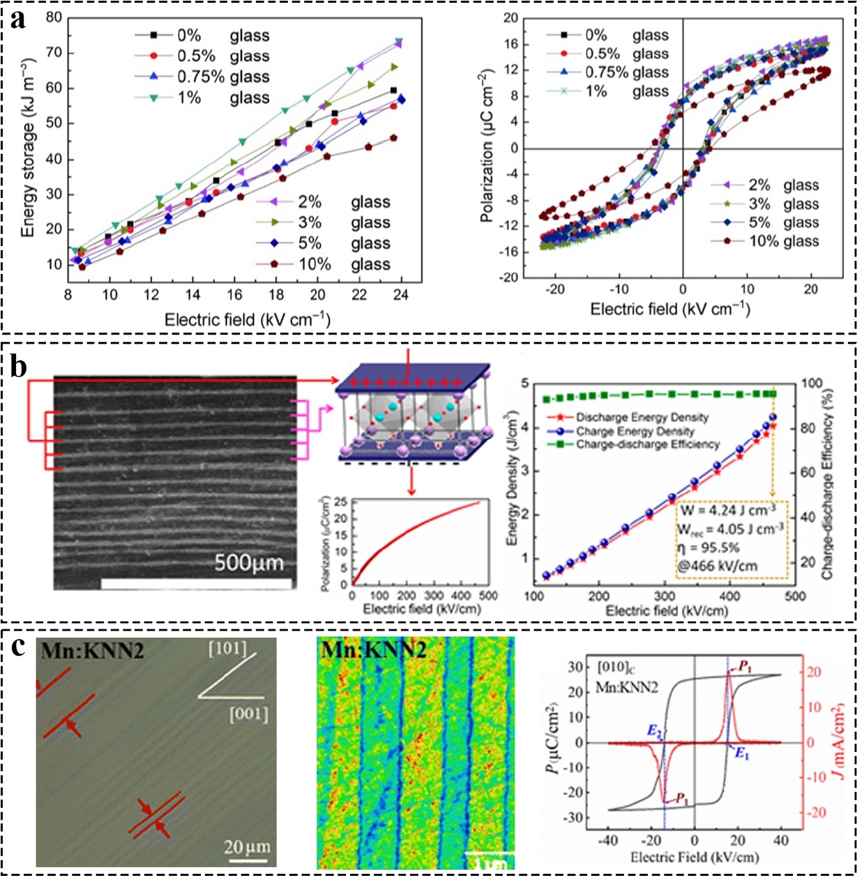
Fig. 2.(a) Dielectric constant (ε
r) and dielectric loss (tan d) according to the frequency of Mn-doped KNLN films with various Mn contents. Raman microprobe spectra of the Mn-doped KNLN films (x = 0, 0.01, 0.02, and 0.03). (Reproduced with permission Ref. [
42]. Copyright, Journal of Materials Science: Materials in Electronics.) (b) P–E Loops of (a) as-grown sample KNMN and (b) post- annealed KNMN film in the RTP at 750°C for 5 min. The atomic force microscopy (AFM) results of the post-annealed KNMN films. (Reproduced with permission Ref. [
43]. Copyright, Journal of the Korean Physical Society.) (c) Field emission-scanning electron microscopy (FE-SEM) surface images of KNN and KNMN thin films, respectively. Polarization (P)-electric field (E) hysteresis loops of a pure KNN and KNMN thin films at as-grown states (Reproduced with permission Ref. [
44]. Copyright, Journal of Materials Science: Materials in Electronics.)
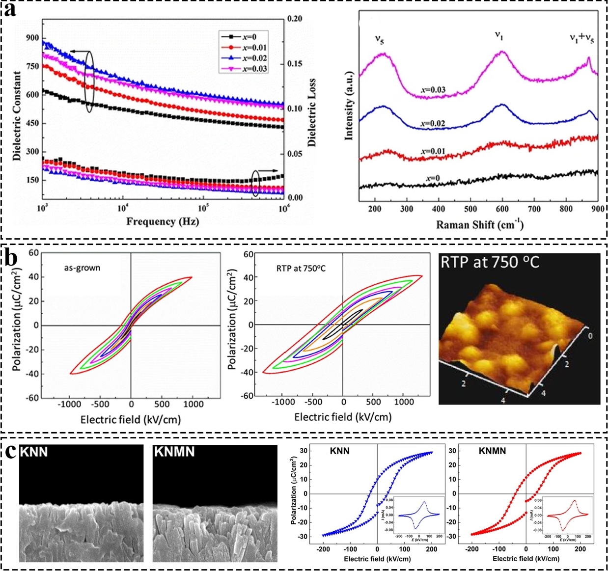
Fig. 3.(a) Frequency dependences of the dielectric constant (ε
r) and dielectric loss (tanδ) for the KNN film and the LKNN film. (Reproduced with permission Ref. [
45]. Copyright, Journal of Advanced Dielectrics.) (b) Room-temperature P-E loops of (1-x) (KNN-BA)-xLi
2O single crystals. (Reproduced with permission Ref. [
46]. Copyright, Journal of Materials Science: Materials in Electronics.) (c) P–I–E loops of (1-x) BNT-xNN ceramics at 9 kV/mm, 10 Hz, 25°C at x = 0.05. (Reproduced with permission Ref. [
58]. Copyright, Journal of the American Ceramic Society.) (d) SEM image of surface morphology of the BCZT ceramic sintered from the powders by sol–gel–hydrothermal process. (e) Ferroelectric hysteresis loops of BCZT ceramic sintered from the powders by sol–gel-hydrothermal process. (Reproduced with permission Ref. [
66]. Copyright, Journal of Materials Science: Materials in Electronics.) (f) FE-SEM images of the (Ba
0.85Ca
0.15) (Ti
0.90Zr
0.10) O
3 ceramics sintered by the spark plasma (Reproduced with permission Ref. [
67]. Copyright, Journal of Materials Science: Materials in Electronics.)
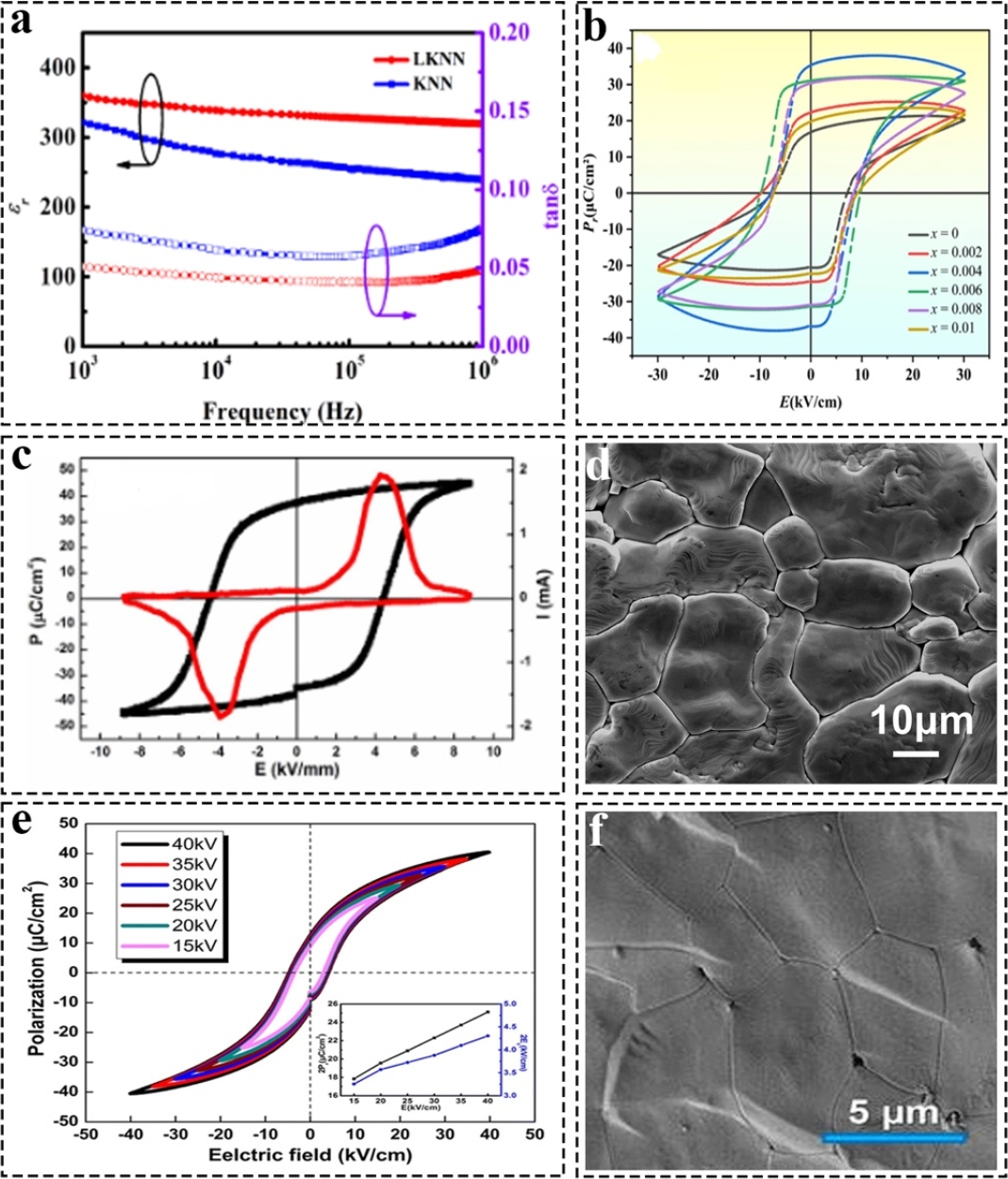
Fig. 4.(a) Schematic illustration of the recrystallization behavior of polymer chains through the solvent vapor annealing process. (Reproduced with permission Ref. [
87]. Copyright, Nano energy.) (b) PVDF-CNT foam with its output performance. (Reproduced with permission Ref. [
88]. Copyright, ACS Applied Materials and Interfaces.) (c) ATR-FTIR spectra and enlarged view (insets) of films in (a) printed with contact to air, vacuum-dried and poled in contact with the positive electrode, (b) printed in contact with glass, vacuum-dried and poled in contact with the negative electrode, and (c) vacuum-dried unpoled. (Reproduced with permission Ref. [
89]. Copyright, RSC Advances.) (d) PE-hysteresis loops of PVDF and composite films: PVDF/Co–P. (Reproduced with permission Ref. [
90]. Copyright, RSC Advances.) (e) FTIR spectra of the produced samples. (Reproduced with permission Ref. [
91]. Copyright, Beilstein Journal of Nanotechnology.) (f) Room temperature XRD patterns of electrospun PVDF-TrFE fiber mats. Online XRD tests were carried out in the temperature range of 25~130°C with a heating rate of 300°C/min (Reproduced with permission Ref. [
92]. Copyright, Nature Communications.)
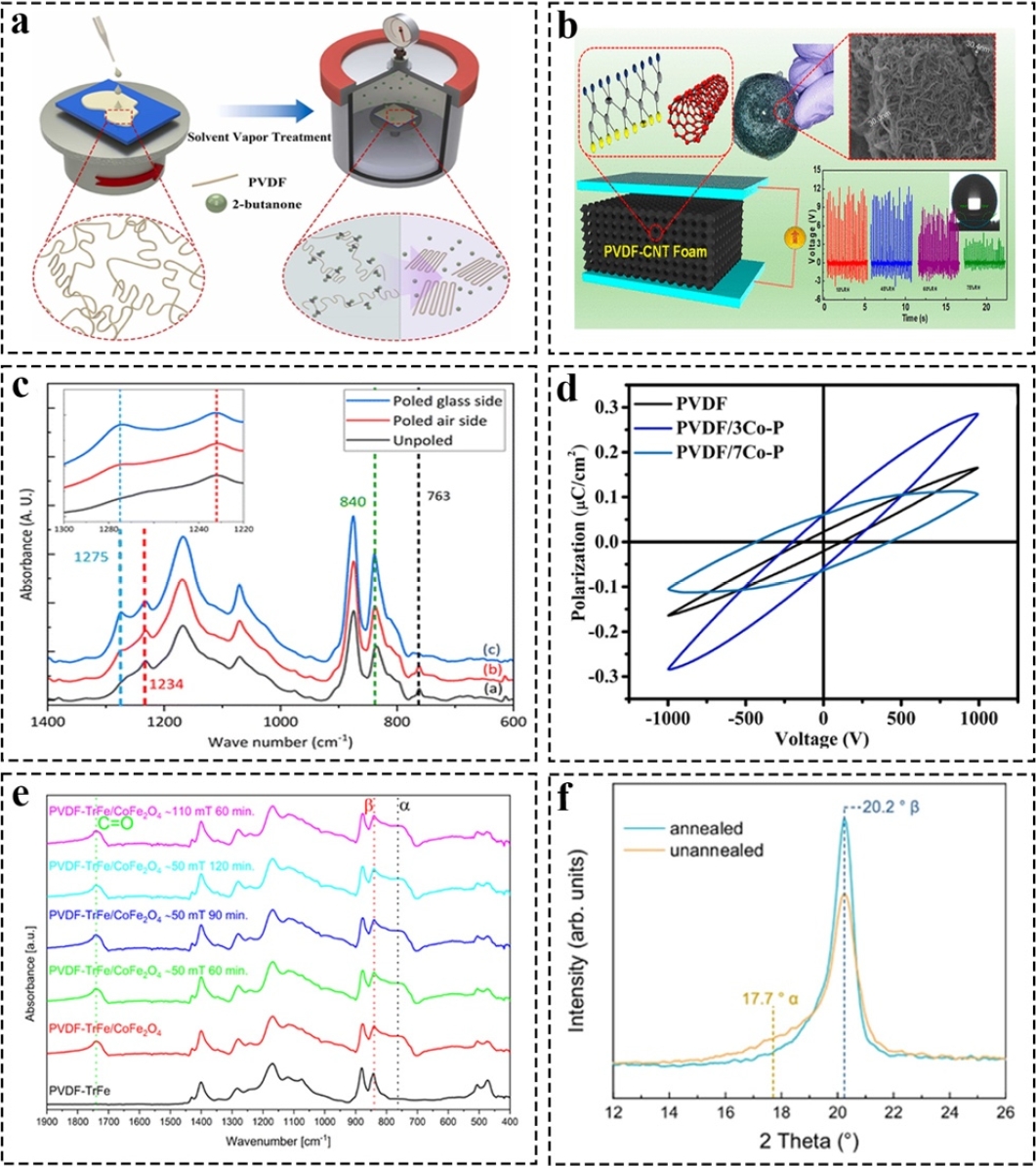
Fig. 5.(a) Nanocomposite thin film prepared by using pristine P(VDF-TrFE) and BTO showing the piezoelectric/triboelectric transduction properties. (Reproduced with permission Ref. [
94]. Copyright, ACS Applied Nano Materials.) (b) The prism/elongated pore morphology of the freeze-cast PVDF with the weight ratio of 0.4/10. (Reproduced with permission Ref. [
99]. Copyright, Soft matter.) (c) Schematic diagrams of the formation mechanism of the micro-porous PVDF structure: Polar solvent (DMSO) and ice-templating induce
α-to-
β transformation via directional chain alignment. (d) FT-IR spectra. (Reproduced with permission Ref. [
100]. Copyright, Sustainable Materials and Technologies.) (e) Aluminum alloy plate with a linear direct-write transducer (DWT) array comprising eight transducers, and sectional view A-A showing layers of the DWT design. (Reproduced with permission Ref. [
105]. Sensors.) (f) The output voltage signal generated by the SS-PF-based f-PEH and commercial PVDF device upon the pump and pipe vibrations in the laboratory (Reproduced with permission. Ref. [
113]. Copyright, Advanced Functional Materials.)
References
- 1. C. Deng, Y. Zhang, D. Yang, H. Zhang, and M. Zhu, Adv. Sens. Res., 3, 2300168 (2024). doi: https://doi.org/10.1002/adsr.202300168
- 2. C. Covaci and A. Gontean, Sensors, 20, 3512 (2020). doi: https://doi.org/10.3390/s20123512
- 3. S. S. Ba Hashwan, M. H. M. Khir, I. M. Nawi, M. R. Ahmad, M. Hanif, F. Zahoor, Y. Al-Douri, A. S. Algamili, U. I. Bature, S. S. Alabsi, M. O. B. Sabbea, and M. Junaid, Discover Nano, 18, 25 (2023). doi: https://doi.org/10.1186/s11671-023-03779-8
- 4. M. Habib, I. Lantgios, and K. Hornbostel, J. Phys. D Appl. Phys., 55, 423002 (2022). doi: https://doi.org/10.1088/1361-6463/ac8687
- 5. A. Khan, R. Joshi, M. K. Sharma, C. J. Huang, J. H. Yu, Y. L. Wang, and Z. H. Lin, Nano Trends, 6, 100032 (2024). doi: https://doi.org/10.1016/j.nwnano.2024.100032
- 6. S. Wang, H. Q. Shao, Y. Liu, C. Y. Tang, X. Zhao, K. Ke, R. Y. Bao, M. B. Yang, and W. Yang, Compos. Sci. Technol., 202, 108600 (2021). doi: https://doi.org/10.1016/j.compscitech.2020.108600
- 7. H. Feng, A. Pang, and H. Zhou, Sci. Rep., 12, 10357 (2022). doi: https://doi.org/10.1038/s41598-022-14332-5
- 8. N. Wang, J. van Turnhout, R. Daniels, C. Wu, J. Huo, R. Gerhard, G. Sotzing, and Y. Cao, ACS Appl. Mater. Interfaces, 14, 42705 (2022). doi: https://doi.org/10.1021/acsami.2c12185
- 9. Q. He and J. Briscoe, ACS Appl. Mater. Interfaces, 16, 29491 (2024). doi: https://doi.org/10.1021/acsami.3c17037
- 10. F. Narita, Z. Wang, H. Kurita, Z. Li, Y. Shi, Y. Jia, and C. Soutis, Adv. Mater., 33, 2005448 (2021). doi: https://doi.org/10.1002/adma.202005448
- 11. M. Pohanka, Biosensors, 15, 197 (2025). doi: https://doi.org/10.3390/bios15030197
- 12. H. Yuan, T. Lei, Y. Qin, and R. Yang, Nano Energy, 59, 84 (2019). doi: https://doi.org/10.1016/j.nanoen.2019.01.072
- 13. A. Sood, M. Desseigne, A. Dev, L. Maurizi, A. Kumar, N. Millot, and S. S. Han, Small, 19, 2206401 (2023). doi: https://doi.org/10.1002/smll.202206401
- 14. K. Tewatia, A. Sharma, M. Sharma, and A. Kumar, Mater. Today Proc., 44, 4548 (2021). doi: https://doi.org/10.1016/j.matpr.2020.10.813
- 15. X. Wang, Y. Zhang, X. Song, Z. Yuan, T. Ma, Q. Zhang, C. Deng, and T. Liang, J. Eur. Ceram. Soc., 32, 559 (2012). doi: https://doi.org/10.1016/j.jeurceramsoc.2011.09.024
- 16. S. Patel, A. Chauhan, and R. Vaish, Energy Technol., 3, 70 (2015). doi: https://doi.org/10.1002/ente.201402118
- 17. H. Yang, F. Yan, G. Zhang, Y. Lin, and F. Wang, J. Alloys Compd., 720, 116 (2017). doi: https://doi.org/10.1016/j.jallcom.2017.05.158
- 18. M. Hjiri, A. Jbeli, N. A. Althumairi, N. Mustapha, and A. M. Aldukhayel, J. Sol-Gel Sci. Technol., 116, 1630 (2025). doi: https://doi.org/10.1007/s10971-025-06948-6
- 19. M. Krupska-Klimczak, P. Gwizd, I. Jankowska-Sumara, D. Sitko, and P. Jeleń, Materials., 15, 5363 (2022). doi: https://doi.org/10.3390/ma15155363
- 20. X. Dong, H. Chen, M. Wei, K. Wu, and J. Zhang, J. Alloys Compd., 744, 721 (2018). doi: https://doi.org/10.1016/j.jallcom.2018.01.276
- 21. G. Liu, L. Zhang, Q. Wu, Z. Wang, Y. Li, D. Li, H. Liu, and Y. Yan, J. Mater. Sci. Mater. Electron., 29, 18859 (2018). doi: https://doi.org/10.1007/s10854-018-0011-3
- 22. Q. Xu, J. Xie, Z. He, L. Zhang, M. Cao, X. Huang, M. T. Lanagan, H. Hao, Z. Yao, and H. Liu, J. Eur. Ceram. Soc., 37, 99 (2017). doi: https://doi.org/10.1016/j.jeurceramsoc.2016.07.011
- 23. T. Wang, H. Zhang, Y. Huang, J. Chen, and W. Gong, J. Alloys Compd., 920, 166035 (2022). doi: https://doi.org/10.1016/j.jallcom.2022.166035
- 24. R. Lang, Q. Chen, T. Gao, J. Zhu, J. Xing, and Q. Chen, J. Eur. Ceram. Soc., 44, 3916 (2024). doi: https://doi.org/10.1016/j.jeurceramsoc.2024.01.004
- 25. N. Kumar, N. Bastola, S. Kumar, and R. Ranjan, J. Mater. Sci. Mater. Electron., 28, 10420 (2017). doi: https://doi.org/10.1007/s10854-017-6813-x
- 26. T. Das, P. Biswas, A. Dev, J. Mallick, and M. Kar, Chem. Eng. J., 479, 147900 (2024). doi: https://doi.org/10.1016/j.cej.2023.147900
- 27. Q. Huang, F. Si, and B. Tang, Ceram. Int., 48, 17359 (2022). doi: https://doi.org/10.1016/j.ceramint.2022.02.299
- 28. F. Si, B. Tang, Z. Fang, H. Li, and S. Zhang, J. Alloys Compd., 819, 153004 (2020). doi: https://doi.org/10.1016/j.jallcom.2019.153004
- 29. Q. Hu, Y. Tian, Q. Zhu, J. Bian, L. Jin, H. Du, D. O. Alikin, V. Y. Shur, Y. Feng, Z. Xu, and X. Wei, Nano Energy, 67, 104264 (2020). doi: https://doi.org/10.1016/j.nanoen.2019.104264
- 30. W. B. Li, D. Zhou, R. Xu, L. X. Pang, and I. M. Reaney, ACS Appl. Energy Mater., 1, 5016 (2018). doi: https://doi.org/10.1021/acsaem.8b01001
- 31. H. Ogihara, C. A. Randall, and S. Trolier‐McKinstry, J. Am. Ceram. Soc., 92, 1719 (2009). doi: https://doi.org/10.1111/j.1551-2916.2009.03104.x
- 32. H. Qi, A. Xie, A. Tian, and R. Zuo, Adv. Energy Mater., 10, 1903338 (2020). doi: https://doi.org/10.1002/aenm.201903338
- 33. J. Wu, D. Xiao, and J. Zhu, Chem. Rev., 115, 2559 (2015). doi: https://doi.org/10.1021/cr5006809
- 34. B. Chen, C. Tao, W. Fan, B. Shen, M. Ju, Z. Dou, C. Wu, F. Z. Yao, W. Gong, and K. Wang, Nanomaterials, 14, 288 (2024). doi: https://doi.org/10.3390/nano14030288
- 35. R. Pinho, R. Vilarinho, J. A. Moreira, F. Zorro, P. Ferreira, M. Ivanov, A. Tkach, M. E. Costa, and P. M. Vilarinho, J. Mater. Chem. C, 11, 7758 (2023). doi: https://doi.org/10.1039/d2tc05538d
- 36. S. Pradhan, M. Rath, A. David, D. Kumar, W. Prellier, and M. S. R. Rao, ACS Appl. Mater. Interfaces, 13, 36407 (2021). doi: https://doi.org/10.1021/acsami.1c05699
- 37. N. Helth Gaukås, S. M. Dale, T. M. Ræder, A. Toresen, R. Holmestad, J. Glaum, M. A. Einarsrud, and T. Grande, Materials, 12, 2042 (2019). doi: https://doi.org/10.3390/ma12132042
- 38. K. N. Pham, N. H. Gaukås, M. Morozov, T. Tybell, P. E. Vullum, T. Grande, and M. A. Einarsrud, R. Soc. Open. Sci., 6, 180989 (2019). doi: https://doi.org/10.1098/rsos.180989
- 39. T. Saito, H. Adachi, and T. Wada, Jpn. J. Appl. Phys., 44, L573 (2005). doi: https://doi.org/10.1143/JJAP.44.L573
- 40. Y. Sun, F. Guo, Q. Lu, and S. Zhao, Ceram. Int., 44, 13994 (2018). doi: https://doi.org/10.1016/j.ceramint.2018.04.250
- 41. Y. Zhang, C. Hu, Y. Wang, X. Huang, X. Sun, M. Liu, B. Xing, X. Wen, and H. Tian, J. Mater. Chem. C, 11, 4837 (2023). doi: https://doi.org/10.1039/d2tc05312h
- 42. X. Zhang, J. Liu, K. Zhu, J. Wang, Z. Li, and J. Qiu, J. Mater. Sci. Mater. Electron., 28, 487 (2017). doi: https://doi.org/10.1007/s10854-016-5547-5
- 43. M. Sheeraz, B. T. Nguyen, H. S. Han, J. S. Bae, S. Cho, T. H. Kim, C. W. Ahn, and I. W. Kim, J. Korean Phys. Soc., 80, 628 (2022). doi: https://doi.org/10.1007/s40042-022-00450-w
- 44. N. D. Phu, X. L. Le, and N. X. Duong, J. Mater. Sci. Mater. in Electron., 35, 1564 (2024). doi: https://doi.org/10.1007/s10854-024-13340-7
- 45. X. Bu, C. Yang, M. Fan, W. Wang, X. Lin, and S. Huang, J. Adv. Dielectr., 13, 2350009 (2023). doi: https://doi.org/10.1142/S2010135X23500091
- 46. Y. Zeng, M. Jiang, X. Liu, T. Wang, Y. OuYang, Y. Xu, S. Cao, J. Song, and G. Rao, J. Mater. Sci. Mater. in Electron., 35, 1510 (2024). doi: https://doi.org/10.1007/s10854-024-13273-1
- 47. N. D. Quan, L. Huu Bac, D. Van Thiet, V. N. Hung, and D. D. Dung, Adv. in Mater. Sci. Eng., 2014, 365391 (2014). doi: https://doi.org/10.1155/2014/365391
- 48. Z. Li, Q. Yang, C. Wang, J. Zhang, Z. Wang, B. Gao, Z. Li, Z. Wang, X. Yan, T. Ai, D. Wang, and Y. Niu, Crystals, 13, 295 (2023). doi: https://doi.org/10.3390/cryst13020295
- 49. S. Supriya, J. Inorg. Organomet. Polym. Mater., 33, 3013 (2023). doi: https://doi.org/10.1007/s10904-023-02765-y
- 50. M. Izumi, K. Yamamoto, M. Suzuki, Y. Noguchi, and M. Miyayama, Appl. Phys. Lett., 93, 242903 (2008). doi: https://doi.org/10.1063/1.3046791
- 51. Y. Li, W. Chen, Q. Xu, J. Zhou, Y. Wang, and H. Sun, Ceram. Int., 33, 95 (2007). doi: https://doi.org/10.1016/j.ceramint.2005.08.001
- 52. Y. Liao, D. Xiao, D. Lin, J. Zhu, P. Yu, L. Wu, and X. Wang, Mater. Sci. Eng. B, 133, 172 (2006). doi: https://doi.org/10.1016/j.mseb.2006.06.026
- 53. B. Wang, L. Luo, F. Ni, P. Du, W. Li, and H. Chen, J. Alloys Compd., 526, 79 (2012). doi: https://doi.org/10.1016/j.jallcom.2012.02.114
- 54. Y. Yuan, S. Zhang, and X. Zhou, J. Mater. Sci. Mater. in Electron., 20, 1090 (2009). doi: https://doi.org/10.1007/s10854-008-9832-9
- 55. Z. Yang, H. Du, L. Jin, and D. Poelman, J. Mater. Chem. A, 9, 18026 (2021). doi: https://doi.org/10.1039/d1ta04504k
- 56. J. Suchanicz, K. Kluczewska-Chmielarz, D. Sitko, and G. Jagło, J. Adv. Ceram., 10, 152 (2021). doi: https://doi.org/10.1007/s40145-020-0430-5
- 57. W. Jia, Y. Hou, M. Zheng, Y. Xu, M. Zhu, K. Yang, H. Cheng, S. Sun, and J. Xing, IET Nanodielectrics, 1, 3 (2018). doi: https://doi.org/10.1049/iet-nde.2017.0003
- 58. Q. Xu, Z. Song, W. Tang, H. Hao, L. Zhang, M. Appiah, M. Cao, Z. Yao, Z. He, and H. Liu, J. Am. Ceram. Soc., 98, 3119 (2015). doi: https://doi.org/10.1111/jace.13693
- 59. D. E. Jain Ruth, M. Muneeswaran, N. V. Giridharan, and B. Sundarakannan, Appl. Phys. A, 122, 502 (2016). doi: https://doi.org/10.1007/s00339-016-0033-8
- 60. M. Zannen, A. Lahmar, H. Khemakhem, and M. El Marssi, Solid State Commun., 245, 1 (2016). doi: https://doi.org/10.1016/j.ssc.2016.07.010
- 61. D. Q. Xiao, D. M. Lin, J. G. Zhu, and P. Yu, J. Electroceramics, 16, 271 (2006). doi: https://doi.org/10.1007/s10832-006-9863-7
- 62. M. Maraj, W. Wei, B. Peng, and W. Sun, Materials, 12, 3641 (2019). doi: https://doi.org/10.3390/ma12213641
- 63. A. Gaur, C. Porwal, I. Boukhris, V. S. Chauhan, and R. Vaish, Materials, 16, 5710 (2023). doi: https://doi.org/10.3390/ma16165710
- 64. M. Anithkumar, A. P. S. Prasanna, N. R. Alluri, and S. J. Kim, Adv. Funct. Mater., 33, 2213907 (2023). doi: https://doi.org/10.1002/adfm.202213907
- 65. M. Anithkumar, A. P. S. Prasanna, N. R. Alluri, T. S. Bincy, K. I. Park, and S. J. Kim, Adv. Compos. Hybrid. Mater., 8, 306 (2025). doi: https://doi.org/10.1007/s42114-025-01386-y
- 66. X. Ji, C. Wang, S. Zhang, R. Tu, Q. Shen, J. Shi, and L. Zhang, J. Mater. Sci. Mater. in Electron., 30, 12197 (2019). doi: https://doi.org/10.1007/s10854-019-01578-5
- 67. X. Yan and B. Peng, J. Mater. Sci. Mater. in Electron., 26, 9649 (2015). doi: https://doi.org/10.1007/s10854-015-3631-x
- 68. W. Liu and X. Ren, Phys. Rev. Lett., 103, (2009). doi: https://doi.org/10.1103/PhysRevLett.103.257602
- 69. W. Li, J. Hao, H. Zeng, and J. Zhai, Curr. Appl. Phys., 13, 1205 (2013). doi: https://doi.org/10.1016/j.cap.2013.03.015
- 70. Y. Zhang, H. Sun, W. Chen, and Y. Li, J. Mater. Sci. Mater. in Electron., 26, 10034 (2015). doi: https://doi.org/10.1007/s10854-015-3684-x
- 71. B. G. Baraskar, Y. D. Kolekar, B. R. Thombare, A. R. James, R. C. Kambale, and C. V. Ramana, Small, 19, 2300549 (2023). doi: https://doi.org/10.1002/smll.202300549
- 72. N. Kumar, R. Kurchania, R. J. Ball, C. R. Bowen, S. K. Mittal, K. L. Yadav, and J. Rani, J. Alloys Compd., 989, 174358 (2024). doi: https://doi.org/10.1016/j.jallcom.2024.174358
- 73. G. S. Kathait, D. Biswas, S. Negi, and S. Maini, Proc. 2024 1st International Conference on Smart Energy Systems and Artificial Intelligence (SESAI) (IEEE, Balaclava, Mauritius, 2024) pp 1 2024, doi: https://doi.org/10.1109/SESAI61023.2024.10599444
- 74. R. Laishram, S. Rajput, and K. C. Singh, J. Alloys Compd., 812, 152128 (2020). doi: https://doi.org/10.1016/j.jallcom.2019.152128
- 75. K. Chandramani Singh, Mater. Lett., 256, 126664 (2019). doi: https://doi.org/10.1016/j.matlet.2019.126664
- 76. N. A. K. Jadoon, V. Puvanenthiram, M. A. H. Mosa, A. Sharma, and K. Wang, Inorganics, 12, 264 (2024). doi: https://doi.org/10.3390/inorganics12100264
- 77. C. L. A. Cunha, T. C. Pimenta, and M. Amorim Fraga, In Thin Films - Deposition Methods and Applications (IntechOpen, London, UK, 2023) pp 1 –17doi: https://doi.org/10.5772/intechopen.106288
- 78. M. Chirumamilla, T. Krekeler, D. Wang, P. K. Kristensen, M. Ritter, V. N. Popok, and K. Pedersen, Appl. Nano, 4, 280 (2023). doi: https://doi.org/10.3390/applnano4040016
- 79. M. K. Sandager, C. Kjelde, and V. Popok, Crystals, 12, 1379 (2022). doi: https://doi.org/10.3390/cryst12101379
- 80. A. Ababneh, U. Schmid, J. Hernando, J. L. Sánchez-Rojas, and H. Seidel, Mater. Sci. Eng. B, 172, 253 (2010). doi: https://doi.org/10.1016/j.mseb.2010.05.026
- 81. Z. Wei, L. Shen, Y. Kuang, J. Wang, G. Yang, and W. Lei, J. Cryst. Growth, 625, 127439 (2024). doi: https://doi.org/10.1016/j.jcrysgro.2023.127439
- 82. T. Vijayakanth, D. J. Liptrot, E. Gazit, R. Boomishankar, and C. R. Bowen, Adv. Funct. Mater., 32, 2109492 (2022). doi: https://doi.org/10.1002/adfm.202109492
- 83. F. Dai, Q. Geng, T. Hua, X. Sheng, and L. Yin, Soft Sci., 3, 7 (2023). doi: https://doi.org/10.20517/ss.2022.30
- 84. X. Liu, Y. Shang, J. Zhang, and C. Zhang, ACS Appl. Mater. Interfaces, 13, 14334 (2021). doi: https://doi.org/10.1021/acsami.1c03226
- 85. N. Soin, T. H. Shah, S. C. Anand, J. Geng, W. Pornwannachai, P. Mandal, D. Reid, S. Sharma, R. L. Hadimani, D. V. Bayramol, and E. Siores, Energy Environ. Sci., 7, 1670 (2014). doi: https://doi.org/10.1039/c3ee43987a
- 86. E. Ghafari, X. Jiang, and N. Lu, Adv. Compos. Hybrid. Mater., 1, 332 (2018). doi: https://doi.org/10.1007/s42114-017-0016-z
- 87. H. Jang, H. J. Park, G. H. Kim, C. M. Kim, N. R. Alluri, B. Bae, H. Jeon, D. Lee, and K. I. Park, Nano Energy, 136, 110705 (2025). doi: https://doi.org/10.1016/j.nanoen.2025.110705
- 88. S. Badatya, D. K. Bharti, N. Sathish, A. K. Srivastava, and M. K. Gupta, ACS Appl. Mater. Interfaces, 13, 27245 (2021). doi: https://doi.org/10.1021/acsami.1c02237
- 89. A. Morali, A. Mandal, M. Skorobogatiy, and S. Bodkhe, RSC Adv., 13, 31234 (2023). doi: https://doi.org/10.1039/d3ra05068h
- 90. C. Bahloul, A. Eddiai, O. Cherkaoui, M. Mazraoui, F. Z. Semlali, and M. El Achaby, RSC Adv., 15, 15218 (2025). doi: https://doi.org/10.1039/d5ra01605c
- 91. M. Fortunato, A. Tamburrano, M. P. Bracciale, M. L. Santarelli, and M. S. Sarto, Beilstein J. Nanotechnol., 12, 1262 (2021). doi: https://doi.org/10.3762/bjnano.12.93
- 92. Y. D. Hu, C. Y. Tang, S. J. Li, Y. J. Wu, K. Ke, R. Chen, C. Luo, Q. X. Dong, H. X. Li, L. Bai, K. Zhang, Y. Wang, Z. Y. Liu, M. B. Yang, and W. Yang, Nat. Commun., 16, 11147 (2025). doi: https://doi.org/10.1038/s41467-025-67292-5
- 93. S. S. Chauhan, U. M. Bhatt, P. Gautam, S. Thote, M. M. Joglekar, and S. K. Manhas, Sens. Actuators A: Phys., 304, 111879 (2020). doi: https://doi.org/10.1016/j.sna.2020.111879
- 94. N. T. Beigh, S. S. Chauhan, and D. Mallick, ACS Appl. Nano Mater., 7, 28106 (2024). doi: https://doi.org/10.1021/acsanm.4c03982
- 95. T. Zhao, Y. Li, and Z. Zhang, Chem. Commun., 62, 3406 (2026). doi: https://doi.org/10.1039/d5cc07179h
- 96. H. Miao, Y. Sun, X. Zhou, Y. Li, and F. Li, J. Appl. Phys., 116, 066820 (2014). doi: https://doi.org/10.1063/1.4891395
- 97. M. Sborikas and M. Wegener, Appl. Phys. Lett., 103, 252901 (2013). doi: https://doi.org/10.1063/1.4850523
- 98. W. Li, Y. Cao, C. Wang, and N. Sepúlveda, Cell. Rep. Phys. Sci., 4, 101388 (2023). doi: https://doi.org/10.1016/j.xcrp.2023.101388
- 99. Y. Zhang, C. R. Bowen, and S. Deville, Soft Matter, 15, 825 (2019). doi: https://doi.org/10.1039/c8sm02160k
- 100. H. Jeon, S. Y. Yoon, N. R. Alluri, M. A. Okirigiti, H. Jang, C. Baek, T. Zhang, G. T. Hwang, M. K. Lee, G. J. Lee, and K. I. Park, Sustain. Mater. Technol., 47, e01888 (2026). doi: https://doi.org/10.1016/j.susmat.2026.e01888
- 101. S. Cha, S. M. Kim, H. Kim, J. Ku, J. I. Sohn, Y. J. Park, B. G. Song, M. H. Jung, E. K. Lee, B. L. Choi, J. J. Park, Z. L. Wang, J. M. Kim, and K. Kim, Nano Lett., 11, 5142 (2011). doi: https://doi.org/10.1021/nl202208n
- 102. J. Ghazanfarian, M. M. Mohammadi, and K. Uchino, Actuators, 10, 312 (2021). doi: https://doi.org/10.3390/ACT10120312
- 103. C. Griffin and V. Giurgiutiu, Sensors, 23, 7103 (2023). doi: https://doi.org/10.3390/s23167103
- 104. M. Ju, Z. Dou, J. W. Li, X. Qiu, B. Shen, D. Zhang, F. Z. Yao, W. Gong, and K. Wang, Sensors, 23, 543 (2023). doi: https://doi.org/10.3390/s23010543
- 105. V. K. Wong, S. M. Rabeek, S. C. Lai, M. Philibert, D. B. K. Lim, S. Chen, M. K. Raja, and K. Yao, Sensors, 22, 5724 (2022). doi: https://doi.org/10.3390/s22155724
- 106. D. S. Aulakh, D. Rawat, and S. Bhalla, Sci. Rep., 15, 36083 (2025). doi: https://doi.org/10.1038/s41598-025-19936-1
- 107. M. J. Yang, G. Y. Gu, and L. M. Zhu, Mechatronics, 24, 724 (2014). doi: https://doi.org/10.1016/j.mechatronics.2014.02.014
- 108. G. Y. Gu and L. M. Zhu, Sens. Actuators A: Phys., 197, 76 (2013). doi: https://doi.org/10.1016/j.sna.2013.03.005
- 109. S. C. Her and H. Y. Chen, Materials, 15, 2027 (2022). doi: https://doi.org/10.3390/ma15062027
- 110. J. Y. Cho, K. B. Kim, W. S. Hwang, C. H. Yang, J. H. Ahn, S. D. Hong, D. H. Jeon, G. J. Song, C. H. Ryu, S. B. Woo, J. Kim, T. H. Lee, J. Y. Choi, H. Cheong, and T. H. Sung, Appl. Energy, 242, 294 (2019). doi: https://doi.org/10.1016/j.apenergy.2019.03.075
- 111. C. K. Jeong, K. I. Park, J. H. Son, G. T. Hwang, S. H. Lee, D. Y. Park, H. E. Lee, H. K. Lee, M. Byun, and K. J. Lee, Energy Environ. Sci., 7, 4035 (2014). doi: https://doi.org/10.1039/c4ee02435d
- 112. Y. Kim, H. Kim, G. J. Lee, H. U. Lee, S. G. Lee, C. Baek, M. K. Lee, J. J. Park, Q. Wang, S. B. Cho, C. K. Jeong, and K. I. Park, Nano Energy, 89, 106469 (2021). doi: https://doi.org/10.1016/j.nanoen.2021.106469
- 113. H. S. Jang, G. H. Kim, D. W. Jeon, H. J. Park, B. N. Bae, N. R. Alluri, C. M. Kim, C. Baek, M. K. Lee, S. B. Cho, G. J. Lee, and K. I. Park, Adv. Funct. Mater., 35, 2415501 (2025). doi: https://doi.org/10.1002/adfm.202415501
- 114. Y. Wang, Y. Yu, X. Wei, and F. Narita, Adv. Mater. Technol., 7, 2200318 (2022). doi: https://doi.org/10.1002/admt.202200318
- 115. A. Wang, M. Hu, L. Zhou, and X. Qiang, Nanomaterials, 8, 1021 (2018). doi: https://doi.org/10.3390/nano8121021
- 116. D. Yu, Z. Zheng, J. Liu, H. Xiao, G. Huangfu, and Y. Guo, Nano-Micro Lett., 13, 117 (2021). doi: https://doi.org/10.1007/s40820-021-00649-9
- 117. W. Guo, C. Tan, K. Shi, J. Li, X. X. Wang, B. Sun, X. Huang, Y. Z. Long, and P. Jiang, Nanoscale, 10, 17751 (2018). doi: https://doi.org/10.1039/c8nr05292a
- 118. X. Ma, X. Liu, X. Li, and Y. Ma, Electronics, 10, 2322 (2021). doi: https://doi.org/10.3390/electronics10192322
- 119. C. Zhao, C. Jia, Y. Zhu, and T. Zhao, Sensors, 21, 5144 (2021). doi: https://doi.org/10.3390/s21155144
- 120. A. Panahi, A. Hassanzadeh, and A. Moulavi, Sens. Bio-Sensing Res., 30, 100378 (2020). doi: https://doi.org/10.1016/j.sbsr.2020.100378