ABSTRACT
Quantum dots (QDs) are semiconductor nanocrystals with sizes on the order of several nanometers, whose bandgaps can be tuned by controlling the particle size. Owing to this bandgap tunability, QDs can absorb near-infrared (NIR) and short-wave infrared (SWIR) light, spectral regions that are difficult to access with conventional silicon-based devices. However, colloidal QDbased infrared photodetectors still suffer from intrinsically high dark current, trap-induced noise, and limited response speed. As a result, they exhibit fundamental performance gaps in terms of detectivity and speed–bandwidth product compared to epitaxial infrared detectors, highlighting the need for structural and architectural design strategies to overcome these limitations. In this review, we discuss recent advances in enhancing the spectral selectivity and sensitivity of infrared photodetectors through three-dimensional optical architectures, including metasurfaces and metamaterials. We focus in particular on design strategies and the underlying mechanisms responsible for performance enhancement, and we outline how structural approaches can be leveraged to effectively control the sensitivity and wavelength selectivity of QD-based infrared detectors.
-
KEYWORDS: Quantum dot, Metasurface, Metamaterial, Infrared photodetector, Quantum dot photodetector
1 Introduction
Colloidal quantum dots (CQDs) are attracting significant attention as a material platform for infrared photodetectors because they are compatible with solution processing and offer widely tunable bandgaps, making them advantageous for low‑cost, large‑area fabrication compared to conventional epitaxial detectors. In particular, IV–VI (PbS, PbSe, HgTe, HgSe) and III–V (InAs, In(As,P), etc.) CQDs can continuously tune their bandgaps from a few hundred nanometers to several micrometers, enabling broadband photodetection across the NIR, SWIR, and MWIR spectral ranges [
1–
6]. These wavelength ranges directly overlap with key application domains such as night vision and thermal imaging for defense and security, LiDAR sensors for autonomous and unmanned vehicles, spectral sensors for industrial process monitoring and gas detection, optical receivers operating at telecommunication wavelengths, and 3D image sensors.
Taken together, these studies indicate that the performance of QD infrared photodetectors is primarily governed by three major axes: (i) the design of the QD materials, surface chemistry, and band structure, (ii) the device architecture (photodiodes, photoconductors, FETs, heterojunctions, etc.) together with the design of charge transport and barrier layers, and (iii) the optimization of the optical path and absorption efficiency. However, in colloidal QD systems the active absorption layer is typically limited to several tens to a few hundreds of nanometers due to constraints in charge transport, film quality, and mechanical integrity, which inherently restricts the total optical absorption that can be achieved within a practical device thickness. In addition, noise and dark current originating from surface traps and ionized impurities, an upper bound in response speed set by the dielectric constant and parasitic capacitance, and thickness/compositional nonuniformities inherent to solution processing all act as fundamental performance limitations.
Because these limitations impose a trade‑off between optical absorption (favoring thicker QD layers) and charge transport/dynamic response (favoring thinner layers), performance saturation often occurs even when the QD material quality and electronic device structure are carefully optimized. In other words, there exists a practical ceiling in detector performance that cannot be overcome by materials and electronic device engineering alone, as further thickening the QD layer to increase absorption leads to excessive series resistance, longer carrier transit times, and larger parasitic capacitance. This intrinsic conflict highlights that, beyond the first two axes, engineering of the optical environment surrounding a given QD layer thickness becomes a crucial additional degree of freedom.
In colloidal QD systems in particular, noise and dark current originating from surface traps and ionized impurities, an upper bound in response speed set by the dielectric constant and parasitic capacitance, and thickness/compositional nonuniformities inherent to solution processing all act as fundamental performance limitations. Because these limitations cannot be completely eliminated by materials and electronic device engineering alone, optical and resonant structure design that maximizes the utilization of incident photons within a limited QD absorption layer thickness has emerged as an essential complementary degree of freedom.
Because these limitations cannot be completely eliminated by materials and electronic device engineering alone, optical and resonant structure design that maximizes the utilization of incident photons within a limited QD absorption layer thickness has emerged as an essential complementary degree of freedom. In particular, plasmonic metasurfaces and metamaterial perfect absorbers provide powerful routes to concentrate, recycle, and spectrally shape the electromagnetic field within ultrathin QD layers without compromising electronic transport, thereby directly addressing the fundamental limitation of insufficient absorption in thin CQD films. In this review, we therefore focus on the third axis — optical and resonant architectures — and systematically summarize how the introduction of plasmonic metasurfaces and metamaterial perfect absorbers can enhance or, in some cases, constrain spectral selectivity, sensitivity, response speed, and angular/polarization selectivity in QD infrared photodetectors. By clearly framing optical and resonant design as a necessary strategy to circumvent the structural limitations of CQD IR photodetectors, we aim to provide a coherent perspective that connects device physics, optical engineering, and practical application requirements.
2 Basic Colloidal QD IR Photodetectors
2.1 Device Operation Mechanism of Colloidal QD IR Photodiodes
In a typical colloidal QD photodetector structure, the QD thin film serves as the primary layer for light absorption and charge generation, while the adjacent electron transport layer (ETL), hole transport layer (HTL), and electrodes are responsible for selectively extracting charges [
7]. The band alignment of the ETL and HTL is engineered to efficiently drive electrons and holes toward opposite electrodes, while the built-in electric field or an external bias suppresses recombination and promotes charge separation [
8].
Charge transport between QDs mainly follows hopping or tunneling mechanisms, and key factors such as interdot spacing, the length and polarity of surface ligands, and the density and ordering of the QD array play critical roles in determining charge mobility and response speed [
9]. Meanwhile, defects and dangling bonds present on QD surfaces and at interfaces form trap states with various energy levels, which temporarily capture photoexcited electrons or holes and thereby induce nonradiative recombination, increased noise, and reduced response speed. These trap-induced effects are particularly pronounced in colloidal QDs and are closely related to device noise characteristics such as dark current and 1/f noise [
10].
From the device-design perspective, intensive efforts have been devoted to strategies that enhance detectivity by reducing trap density through the introduction of core/shell structures, surface passivation, and ligand engineering, and by blocking dark-current pathways using architectures such as p–n junctions, p–i–n structures, and double-barrier structures [
11]. Consequently, the performance of QD photodetectors is governed not only by the intrinsic light-absorption properties of the QDs themselves, but also by a combination of structural and electrical factors such as interfacial band alignment, the distribution of trap states, and the design of charge-transport layers and electrodes.
Therefore, to realize high-performance QD photodetectors, it is essential to understand the operating mechanisms from a multilayered design perspective encompassing materials, interfaces, and device architecture, and to quantitatively identify loss mechanisms at each stage. Recently, III–V and IV–VI colloidal QD photodiodes have achieved a considerable level of performance in terms of cutoff wavelength, quantum efficiency, dark current, and response speed even without additional cavities or metasurfaces. In this chapter, we summarize the performance and design strategies of such basic devices and aim to establish a reference point for comparing the additional performance enhancements that can be expected when metasurface and metamaterial structures are integrated.
2.2 Device Performance of Colloidal QD IR Photodiodes
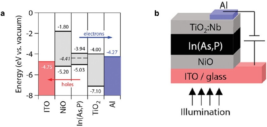
Leemans et al. demonstrated a short-wave infrared (SWIR) photodiode capable of operating up to 1,400 nm using In(As,P) CQDs. They synthesized three sizes of In(As,P) QDs with band edges at 1,140, 1,270, and 1,400 nm, respectively, and formed ntype CQD thin films via short-chain ligand exchange. A sandwich structure was then constructed using p-NiO and Nb:TiO₂ as the hole and electron transport layers, respectively (
Fig. 1a,
b). As a result, each device exhibited an internal quantum efficiency of approximately 46% near the QD bandgap and achieved significant sensitivity in the SWIR region up to 1,400 nm.
In III–V CQD-based NIR photodetectors, improving response speed has been proposed as an important design objective [
12]. In the Fast Near-Infrared Photodetection study, the surface of InAs CQDs was treated with amphoteric ligands to simultaneously passivate both In and As dangling bonds, achieving high carrier mobility (0.04 cm² V⁻¹ s⁻¹) along with a low dielectric constant. As a result, the photodiode maintained an external quantum efficiency (EQE) of about 30% at 940 nm, while exhibiting a response time faster than 2 ns — one of the fastest ever reported among CQD photodiodes [
13].
Meanwhile, PbS and PbSe-based CQD photodetectors remain among the most mature technologies, offering advantages such as high absorption coefficients, relatively simple synthesis, and a broad detection wavelength range. For example, several studies have proposed strategies to suppress dark current in SWIR photodiodes based on PbS CQDs by optimizing the combination of barrier and charge transport layers. Through this approach, devices achieved both low dark current—suitable for highresolution imagers—and sufficient detectivity [
3,
14–
16].
As described above, colloidal QD infrared photodetectors have already achieved high quantum efficiency, fast response speed, and low dark current in the SWIR/NIR regions through advances in material and surface chemistry, device architecture, and interface engineering, substantially elevating the benchmark for electronic performance metrics. Nevertheless, the QD absorption layer thickness—limited to several tens to hundreds of nanometers—and the resulting insufficient light absorption remain fundamental constraints [
17–
23]. To further enhance the sensitivity and spectral selectivity of CQD devices beyond these limits, a structural approach that integrates optical design elements such as resonant cavities, metasurfaces, or metamaterials is essential [
24,
25].
3 Metasurface-Enabled Optical and Resonant Structure Design for QD Photodetectors
As discussed in the previous section, the thickness of the QD photodetector’s absorption layer is often limited to several tens to hundreds of nanometers due to considerations of charge transport and recombination. However, such a limited thickness makes it difficult to achieve sufficient light absorption, particularly in the SWIR and MWIR regions. Consequently, extensive research has focused on optical structures that extend the optical path length or enhance the local electric field through resonance effects [
26–
32]. These structures include metamaterial perfect absorbers, plasmonic metasurfaces, and dielectric metasurfaces, which, when integrated with the QD layer, enable simultaneous control of various performance parameters such as spectral selectivity, sensitivity, directionality, and polarization selectivity [
33,
34].
A metamaterial perfect absorber is an artificially engineered periodic structure designed to absorb nearly 100% of incident electromagnetic waves at specific wavelengths or frequencies by simultaneously minimizing both reflection and transmission. Typically, a metamaterial perfect absorber has a metal–insulator– metal (MIM) stack configuration, in which the bottom metal layer blocks transmission while the coupling resonance between the top metasurface pattern and the ground metal layer suppresses reflection at the target wavelength.
The advantages of such a perfect absorber design include maintaining high absorption over a relatively broad spectral range, the ease of integrating optical functionality with electrodes and interconnects into a single metasurface, and the ability to fabricate it using relatively simple CMOS-compatible patterning processes [
35–
39].
3.1.1 Operation Principles and Representative CQD Implementations
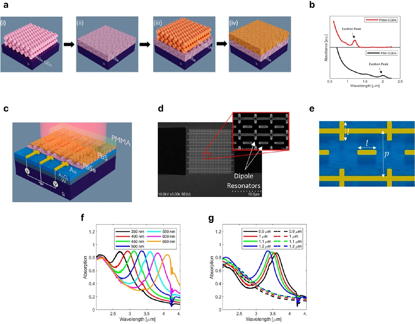
To clarify how metasurface and metamaterial designs modify the light–matter interaction in CQD photodetectors, the planar reference structure is first summarized (
Fig. 2a,
b). The fabrication of the annealed PbSe/PbS CQD bilayer stack used as the photoconducting heterojunction is illustrated in the schematic (
Fig. 2a), and the absorption spectra of PbSe and PbS CQDs in solution are shown in the accompanying plot, highlighting the excitonic peaks due to quantum confinement and the absence of absorption beyond 2 μm (
Fig. 2b). Together, these panels underscore that a planar CQD layer has a limited physical thickness and therefore a limited single-pass optical path, so that mid-IR absorption must be enhanced by engineering the solid-state film and its optical environment rather than relying on solution-phase absorption alone.
Schwanninger et al. reported a PbSe/PbS CQD-based mid-IR photodetector that represents a prominent example of combining such a CQD heterojunction with a metamaterial perfect absorber. In their work, a metallic metasurface perfect absorber was designed and integrated on top of the sintered PbSe/PbS heterojunction photoconductor stack, yielding strong absorption and photoresponse over the 2,710–4,250 nm wavelength range. In this architecture, the top metallic metasurface goes beyond the role of a simple electrode by supporting a strong resonant mode at specific wavelengths that concentrates the incident electromagnetic field inside the CQD layer, thereby simultaneously enhancing both optical absorption and photocurrent generation. A schematic of the resulting metamaterial-enhanced PbSe/PbS CQD heterojunction photodetector under top illumination is shown, in which a W/Al2O3/Au metal–insulator–metal stack forms the metasurface cavity while also serving as the top contact and a PMMA overlayer provides passivation (
Fig. 2c).
The SEM and schematic top-view images reveal that the metasurface pattern consists of freestanding dipole resonators formed in the top Au layer and metallic lines connecting them, with the resonator length
l and lattice period
p used as the key design parameters (
Fig. 2d,
e). Examination of the passive absorption spectra shows how these parameters tune the resonance: increasing
l at fixed
p = 1.2
μm shifts the absorption peak toward longer wavelengths, whereas varying
p at fixed
l = 500 nm induces systematic blue- or redshifts of the resonance peak (
Fig. 2f,
g). This demonstrates that the resonance wavelength and bandwidth of the metamaterial perfect absorber can be precisely engineered through
l and
p, allowing the absorption peak to be aligned with a desired mid-IR wavelength range and structurally matched to the spectral response of the CQD photodetector.
Comparative measurements of responsivity, detectivity, and EQE quantitatively demonstrate the performance enhancement in the metamaterial-integrated structure: the responsivity of the metamaterial-integrated device exhibits an increasingly larger enhancement with wavelength compared with the reference photoconductor at the same wavelength, reaching roughly a tenfold increase for certain designs. When combined with the ∼2-fold improvement provided by the PbSe/PbS heterojunction, the final structure achieves an overall ∼20-fold enhancement in responsivity relative to the reference single PbSe QD photoconductor, while the detectivity also increases simultaneously at multiple wavelengths, indicating that not only the absorption but also the photocarrier collection efficiency has been improved through the design of the resonant structure and electrode/contact engineering.
3.1.2 Practical Limitations and Design Trade‑Offs
Metamaterial perfect absorbers have attracted significant attention because they can achieve nearly perfect absorption at specific wavelengths; however, they also entail several limitations in terms of practical application and scalability. First, their reliance on precise subwavelength-scale nanopatterning leads to high process complexity and cost, making it difficult to scale to large-area fabrication and mass production. In addition, because the resonance condition is highly sensitive to the size, spacing, and thickness of the meta-atoms, even slight process errors or material nonuniformities can cause substantial variations in the absorption wavelength and efficiency, which poses a major constraint.
By contrast, issues such as strong metallic losses and the associated heat generation, incidence-angle dependence, and the potential increase in thermal noise due to excessive absorption must also be carefully considered as key limiting factors. Therefore, when applying a metamaterial perfect absorber to QD photodetectors, it is necessary at the design stage to carefully determine how closely one should pursue the ideal perfect-absorption condition, taking into account the target wavelength bandwidth, operating temperature, operating bias, and acceptable dark current in the intended application environment [
40,
41].
A plasmonic metasurface is an artificial structure that manipulates the phase, amplitude, polarization, and spectral response of light on a two-dimensional plane by precisely controlling surface plasmon resonances through arrays of subwavelength-scale metallic nanostructures. Compared with bulk metamaterials, such metasurfaces are significantly thinner yet provide strong local electromagnetic field enhancement and highly tunable scattering and absorption, making them particularly advantageous for the design of ultrathin optical devices [
42,
43].
By tailoring the shape, size, and array period of the metallic nanoantennas, as well as the refractive index at the metal–dielectric interface, it is possible to realize selective resonant responses for specific wavelengths and polarization states. Building on this capability, intensive research has been conducted on implementing a variety of functional optical components, including planar lenses, polarization elements, color filters, and perfect absorbers [
44–
47].
3.2.1 Resonant Enhancement Mechanisms and Device Demonstrations
The paper Metasurface Colloidal Quantum Dot Photodetectors demonstrates that integrating a metasurface with colloidal QD photoconductors and photodiodes optimized for wavelengths around 1,550 nm can greatly enhance absorption and responsivity. By designing a nanoantenna-array metasurface on top of a QD layer with a thickness of approximately 75 nm, they achieved about a tenfold increase in absorption compared with a planar QD thin film of the same thickness. As a result, the photoconductor structure exhibited a maximum responsivity of about 8,000 A/W and a low NEP on the order of several tens of pW/Hz½, while the photodiode structure showed a responsivity of roughly 5 mA/W and a rise time of about 14 μs [
25].
In addition, several studies have consistently reported that, in the SWIR/NIR region, when one aims to achieve high responsivity even with an ultrathin QD absorption layer (on the order of several tens of nanometers), device architectures that combine nanoantenna metasurfaces for local electric field enhancement with a photo-gain mechanism are particularly effective [
3,
48,
49]. Enhancing the performance of QD photodetectors using plasmonic structures is also being actively pursued.
Metallic nanostructures such as gold nanorods, crescents, and splitring resonators (SRRs) can strongly amplify the electric field in the vicinity of the QD layer via localized surface plasmon resonances (LSPRs). In a study combining PbS/CdS QDs with a plasmonic crescent metasurface, a substantial enhancement of photoluminescence was observed in the telecom wavelength range, suggesting that using the same structure as an absorber layer could lead to improved absorption and responsivity in photodetectors. In another example, where a gold nanorod-based plasmonic structure was incorporated into an HgTe QD photodiode, the photocurrent and detectivity were significantly enhanced at the resonance wavelength, and design conditions were identified that enable simultaneously high responsivity and low noise in a specific MWIR wavelength range [
23].
Among the various types of plasmonic metasurfaces, structures that support quasi-BIC modes are characterized by symmetryengineered resonances that are designed to couple only weakly to free-space radiation modes, and a small symmetry-breaking perturbation is then introduced to simultaneously achieve extremely high Q-factors and strong field enhancement.
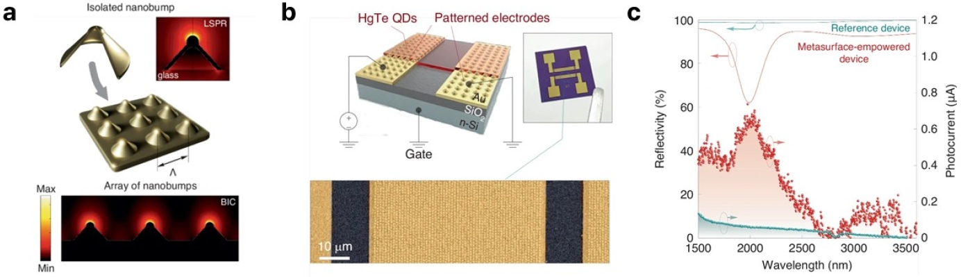
In a structure where HgTe QDs are integrated on top of a laserprinted array of gold nanobumps (
Fig. 3a,
b), the quasi-BIC mode leads to more than a tenfold enhancement of photoluminescence at specific wavelengths, and a pronounced change in emission directionality is observed depending on the collection numerical aperture. Such quasi-BIC-based designs have the potential, when applied to photodetectors, to maximize absorption and photocurrent within an ultranarrow spectral band.
In addition, the nanobump array suppresses optical losses due to reflection while concentrating the incident light into the QD active layer, thereby enabling efficient conversion into electrical signals (
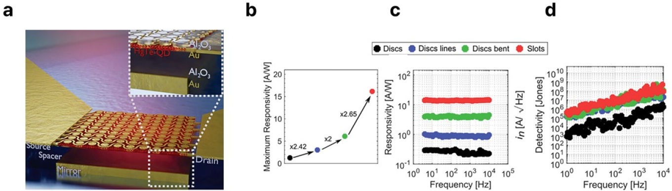
Fig. 3c). From a design perspective, the key parameters include the lattice constant that matches the resonance period to the wavelength, the symmetry that forms the BIC and the degree of asymmetry that breaks it, the separation and dielectric thickness between the QD layer and the metasurface, and the overlap between the hotspot locations and the QD active region. Since an overly sharp resonance becomes sensitive to fabrication tolerances and variations in the angle of incidence, it is important in practical device design to balance the Q factor against process tolerances. For HgTe colloidal QD-based metamaterial photodetectors (
Fig. 4a), Schwanninger et al. showed that systematic optimization of the metamaterial geometry can simultaneously yield large improvements in responsivity and detectivity. By employing a metamaterial design with narrow slot widths, they reduced the active QD volume while maintaining near-unity absorption over almost a single period, and, together with optimized contact engineering to enhance photocarrier collection efficiency, they achieved about a 13-fold increase in responsivity and an approximately 345-fold increase in detectivity at 2,710 nm.
The final device exhibited a responsivity of 16.2 A/W and a specific detectivity of 6 × 10⁸ Jones at 2,710 nm (
Fig. 4b–
d), clearly demonstrating that, in metamaterial design, it is crucial to consider not only absorption but also active-layer volume and noise characteristics [
50].
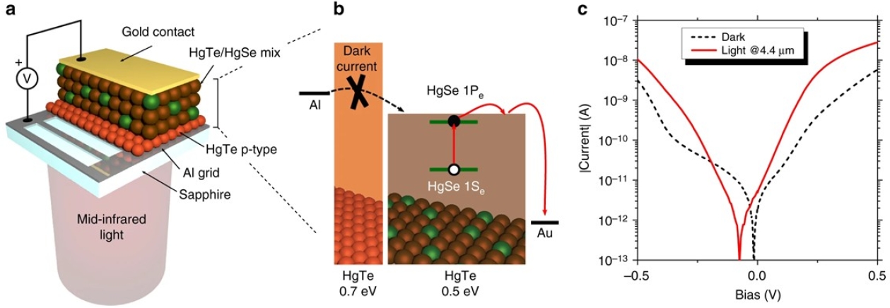
In addition to optical structure design, approaches that engineer the QD layer itself as a kind of metamaterial are also important for improving the performance of infrared photodetectors. The HgSe/HgTe mixed colloidal quantum dot IR photodetector (CQDIP) structure (
Fig. 5a,
b) proposed by Livache et al. is an example in which the concept of wavefunction engineering, originally employed in epitaxial quantum well and quantum dot infrared photodetectors, is extended to colloidal QD systems. In their work, intraband-absorbing HgSe nanocrystals were mixed with lightly doped HgTe nanocrystals to design an energy profile in which a single mixed layer simultaneously plays the roles of both the absorbing region and the barrier layer.
As a result, they maintained intraband absorption in the MWIR region while achieving low dark current, high activation energy, and fast response, reporting a detectivity of about 1.5 × 10⁹ Jones and a response time below 500 ns at 80 K (
Fig. 5c) [
51].
Such QDIP “metamaterial” designs represent a strategy for controlling charge transport and recombination by finely tailoring the energy landscape through appropriate combinations of QD composition, size, doping level, and layer thickness, independently of the optical structure. Going forward, it is expected that research will increasingly focus on combining such wavefunction engineering with plasmonic and dielectric metasurface structures, in order to simultaneously optimize both the absorber–barrier design and the resonant optical architecture.
3.2.2 Limitations of Plasmonic Metasurfaces
Plasmonic metasurfaces offer strong local electromagnetic field enhancement and precise subwavelength wavefront control, but they also inherently suffer from limitations arising from metal losses. Ohmic losses in metallic nanostructures not only degrade the resonance quality factor (Q-factor) but also cause most of the absorbed optical energy to dissipate as heat, which restricts the practical efficiency for photoelectric conversion or nonlinear processes.
In addition, because the resonance wavelength and phase response are highly sensitive to the size, shape, spacing of the nanostructures and to the refractive index at the interfaces, spectral shifts and performance instabilities can easily occur due to fabrication variations or environmental changes, posing significant challenges to scaling toward large-area, high-throughput manufacturing. From the standpoint of spectral, angular, and polarization response, plasmonic metasurfaces typically exhibit narrowband resonances with strong dependence on polarization and incidence angle, and it remains difficult to realize, within a single structure, simultaneous broadband operation, multi-band functionality, and angular- and polarization-insensitive behavior.
Moreover, in the visible and near-infrared regimes, the effective loss of metals increases and practical limits on fabrication resolution become more severe, making it challenging to reproduce theoretically predicted performance in real devices. For these reasons, the introduction of low-loss or nonplasmonic alternative materials, hybrid architectures that combine plasmonic elements with dielectric metasurfaces or active media, and robust design strategies tolerant to fabrication imperfections remain key issues that must be addressed in future plasmonic metasurface research [
52,
53].
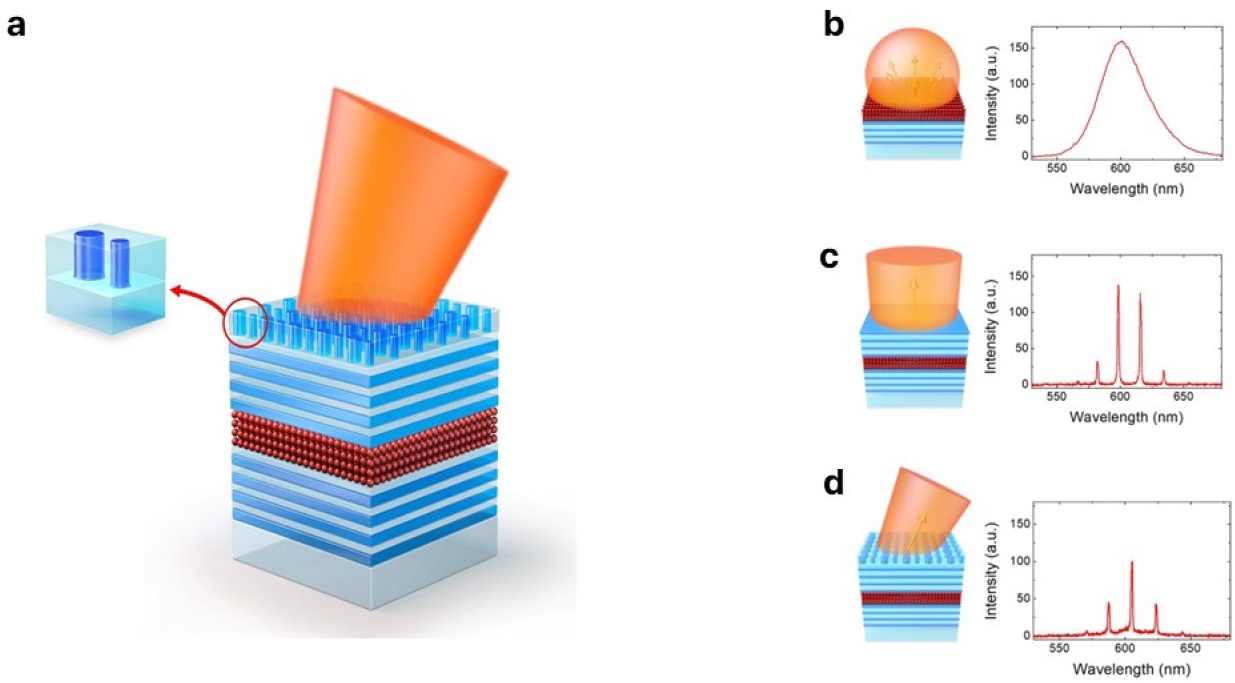
Controlling the directionality of QD emission and absorption using three-dimensional optical structures is also an important research direction. Park et al. proposed a structure in which colloidal QDs are stacked on a dielectric metasurface (
Fig. 6a) composed of an array of high-refractive-index TiO
2 nanodisks, thereby concentrating QD emission into specific forward radiation angles via Mie resonances.
In this structure, they demonstrated that the radiation pattern and spectrum can be precisely tuned by adjusting the diameter, height, and period of the metasurface (
Fig. 6b–
d), achieving an 18° deflection with a deflection efficiency of ~71%. This work, although demonstrated in an emissive configuration, provides a useful design strategy for shaping the angular response and effective numerical aperture of collection/emission optics in integrated optical systems and for reducing inter-channel crosstalk in multichannel imaging systems [
54]. From a detector perspective, the same metasurface phase-engineering concept can be inverted to preferentially couple incident photons from selected angles into the QD absorption layer, thereby realizing compact angle-sensitive photodetectors without bulky external optics.
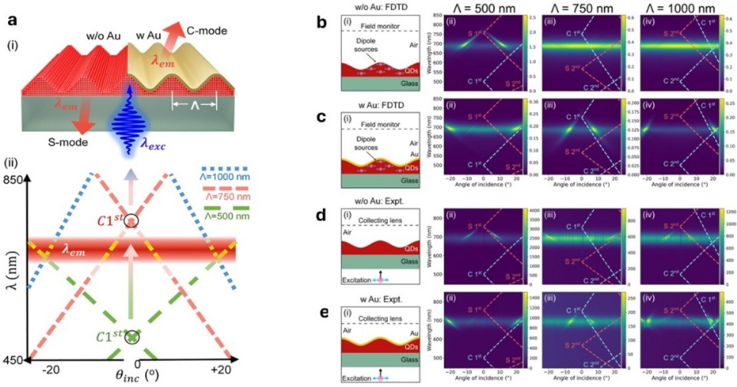
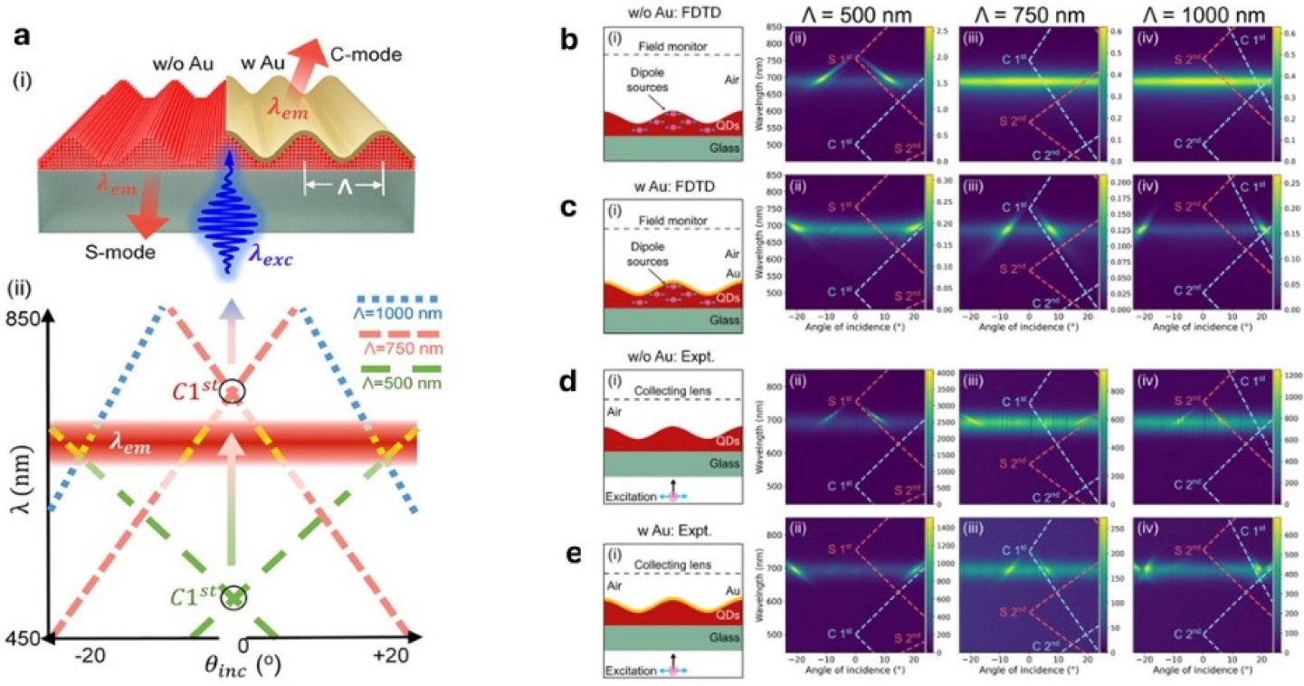
In the study on selective directional enhancement using gold/perovskite QD metasurfaces, a gold metasurface was formed on top of a perovskite QD layer and designed so that the photoluminescence (PL) is selectively enhanced at specific wavelengths and emission angles (
Fig. 7a), thereby demonstrating simultaneous control of the emission directionality and spectrum (
Fig. 7b–
e). This approach can be applied not only to QD lightemitting devices but also, conversely, to QD photodetectors, where it can be used to precisely tailor the response to incident light as a function of angle of incidence, polarization, and wavelength [
55]. While this work focuses on QD light-emitting metasurfaces, the underlying resonant coupling and diffraction physics can be directly exploited in QD photodetectors: by reversing the direction of light propagation, identical metasurface geometries can shape the detector responsivity with respect to incidence angle, polarization, and wavelength, enabling compact angle- and polarization-selective imaging pixels without bulky macroscopic optics. Furthermore, recent demonstrations of gradient-metasurface directional photodetectors confirm that integrating phase-gradient plasmonic metasurfaces on planar devices produces sharp, tunable peaks in the angular response, experimentally validating that metasurface-based directionality control can be translated from emission engineering to practical detector architectures [
56].
A comparison of the QD metastructure integrated photodetectors reported to date shows that the primary performance metrics improved can be broadly classified according to the type of structure employed. Plasmonic metasurfaces and quasi-BIC structures are advantageous for greatly enhancing responsivity at specific wavelengths through narrowband spectral selectivity and strong field enhancement, and they are also well suited for simultaneously achieving directional and polarization-selective responses. Metamaterial perfect absorbers provide high absorption and responsivity over a relatively broad wavelength range and facilitate the integration of electrodes and optical functionality, which is beneficial for system-level implementation. Dielectric metasurfaces and photonic structures, on the other hand, avoid metal losses while enabling fine control of radiation patterns and incidence-angle response via phase and wavefront engineering, making them suitable for applications that demand high-speed operation and low loss. In this context, emission-based demonstrations of directional QD metasurfaces should be viewed as experimentally convenient platforms that reveal how metasurface geometry controls the redistribution of optical power in angle and polarization space, which in turn provides direct and quantitative design guidelines for next-generation angle- and polarization-sensitive QD infrared photodetectors.
4 Conclusion
In this review, we have summarized recent studies on the materials, device architectures, and optical design of colloidal quantum dot– based infrared photodetectors, with a particular focus on strategies that enhance sensitivity and spectral selectivity through threedimensional optical structures incorporating metasurfaces and metamaterials. The fundamental limits of QD IR photodetector performance are set by the band structure and surface chemistry of the QDs, as well as by device architecture and interface engineering, but numerous examples have shown that, within an absorption layer of inherently limited thickness, how efficiently incident photons are utilized is strongly governed by the design of the optical path and resonant structures. Looking ahead, the design of QD-based infrared photodetectors should move away from ranking different meta-architectures by a single figure of merit, and instead adopt multi-criteria optimization tailored to the target application—such as high-sensitivity single-color sensors, multichannel/hyperspectral imagers, high-speed communication receivers, and polarization/angle-sensitive detectors—taking into account the required spectral bandwidth, collection angle, acceptable noise level and operating temperature, and target response speed.
Notes
-
Acknowledgement
This work was supported by a New Faculty Research Grant of Pusan National University, 2023.
-
Conflict of Interest
The authors have no conflicts of interest to declare.
-
Author Contributions
Min Jeong Kim: Investigation, Writing - Original Draft, Writing.
Tae Won Nam: Review & Editing, Supervision.
Data Availability
Data sharing not applicable – no new data generated.
Fig. 1.(a) Energy level diagram of the In(As,P) QDPD stack used here. The diagram was constructed by combining UPS results for the 1140 In(As,P) QD film and literature data for the contact materials. (b) Schematic of the QDPD stack (Adapted from Ref. [
12], licensed under CC BY 4.0 (© The Authors 2022, published by Wiley-VCH))
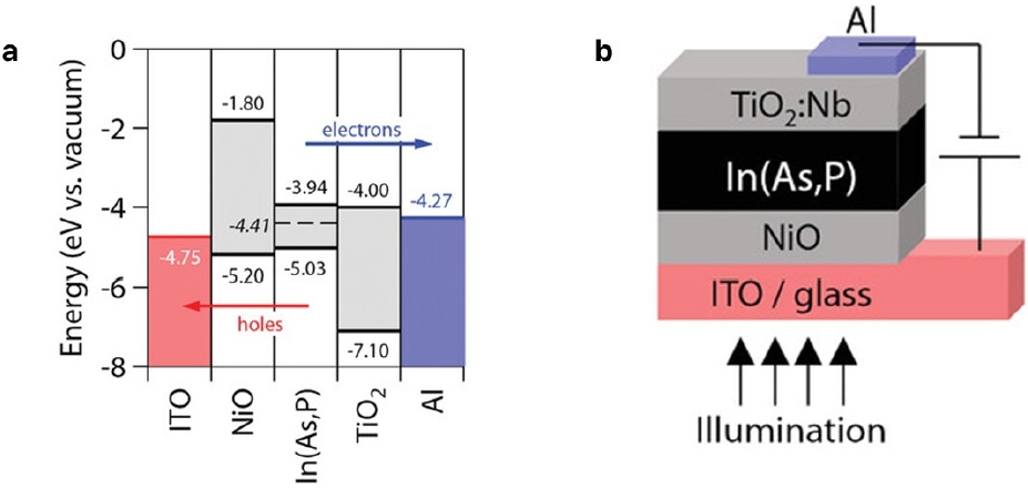
Fig. 2.(a) Illustration of the fabrication of the annealed PbSe/PbS bilayer stack layers as used for the GIXRD (grazing incidence X-ray diffraction) characterization. (i) Solution deposited PbSe CQDs on Si substrate after annealing, at 130°C for 1 min. (ii) Sintered PbSe layer after elevated temperature annealing at 310°C for 1 min. (iii) Solution deposited PbS CQDs on the sintered PbSe CQD layer. (iv) Sintered PbSe/PbS bilayer stack after second elevated temperature annealing, 310°C for 1 min. (b) UV–vis absorbance spectra, in arbitrary units, of CQDs in solution, showing absorbance peaks resulting from the quantum confinement and no absorbance for wavelengths larger than 2 μm. This plot shows the general shape of the absorption curve of the CQDS in solution and is not an absolute measure. (c) Schematic of the metamaterial-enhanced PbSe/PbS CQD heterojunction photodetector under top illumination. A W/Al2O3/Au metal–insulator–metal stack forms the metasurface, which enhances absorption and provides the top contact to the PbSe/PbS photoconducting layer, while a thin PMMA overlayer ensures passivation. (d) SEM image of the metamaterial design showing the Au top layer with the freestanding and interconnected resonating elements. (e) Top view of the designed metamaterial with the contact lines and dipole resonators including the design parameters. (f) Passive absorption spectra of metamaterial detector. The resonator lengths l were varied and the period was kept constant at p = 1.2 μm. The absorption peaks shift toward larger wavelengths when increasing the dipole resonator length l. (g) Passive absorption spectra of metamaterial detectors (Adapted with permission from Ref. [
34]. Copyright 2023 American Chemical Society)
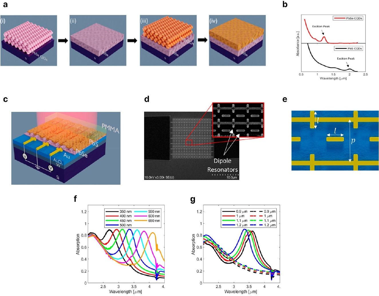
Fig. 3.(a) Sketch of an isolated nanobump and its ordered arrays, as well as calculated intensity distribution upon excitation of the LSPR in the isolated structure (at λR = 2.54 μm) and BIC mode in the array of such structures (at λR = 1.47 μm). The following parameters of the nanobump were used for simulations: height of 0.42 μm, the base radius of 0.4 μm and pitch size of Λ = 1.2 μm. (b) A 3D sketch, optical and false-color SEM image of the plasmonic nanobump array laser-printed on the drain and source contacts of the FET. (c) Reflection (solid curves) and photocurrent spectra (markers) of the HgTe QD photodetector with smooth (green) and patterned (red) Au electrodes (Adapted from Ref. [
8], licensed under CC BY 4.0)
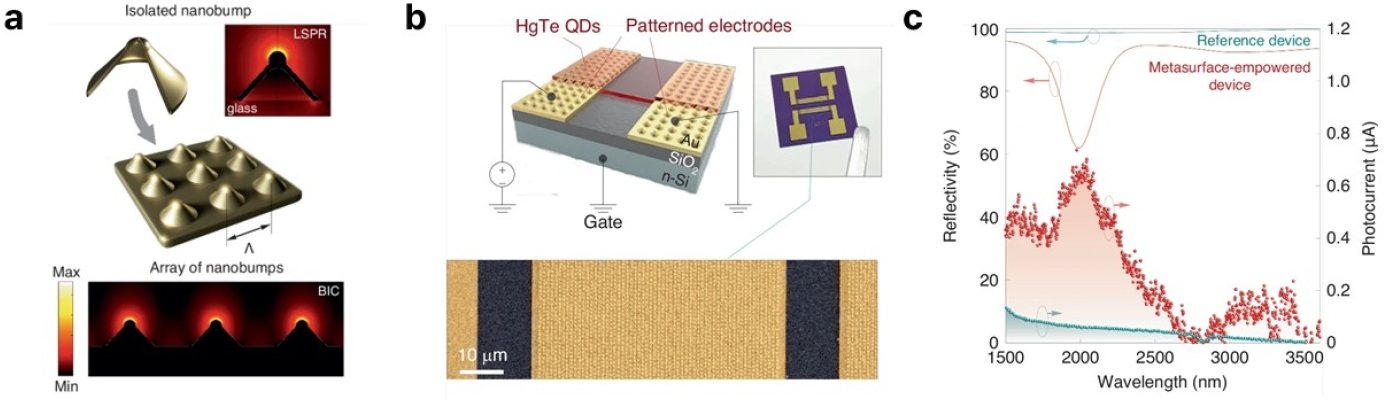
Fig. 4.(a) Illustration of a metamaterial enhanced HgTe photodetector with source and drain contacts. The detectors consist of a 100 nm Au back reflector (Mirror), a 17.5 nm alumina spacer layer (Spacer), followed by 60 nm thick Au resonator with 5 nm alumina on top. The resonator layer is embedded in a ≈ 60 nm HgTe layer that is covered by 120 nm PMMA nm layer for passivation. For comprehensibility the CQD layer was only infilled between the resonators and the PMMA was omitted in the main image. (b) Maximum responsivity of the four different metamaterials. (c) Frequency dependent responsivity of typical metamaterial devices. (d) Detectivity versus frequency (Adapted from Ref. [
50], licensed under CC BY 4.0 (© The Authors 2024, published by Wiley-VCH GmbH))
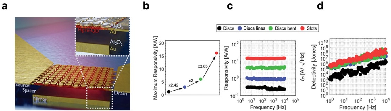
Fig. 5.Design of an intraband photodiode from a colloidal quantum dot infrared photodetector. (a) Scheme of the device. Illumination is provided from the back side through a sapphire substrate and a patterned aluminum electrode allowing 70% of light transmission in the mid-infrared. (b) Band alignment diagram of the diode structure. HgTe 6k is used as a unipolar barrier to filter injection of dark current into the active HgSe/HgTe 4k layer. (c) I(V) characteristics of the device measured at 80 K in the dark and in front of a 4.4-μm quantum cascade laser (Adapted from Ref. [
51], licensed under CC BY 4.0 (© The Authors 2019, published by Springer Nature))
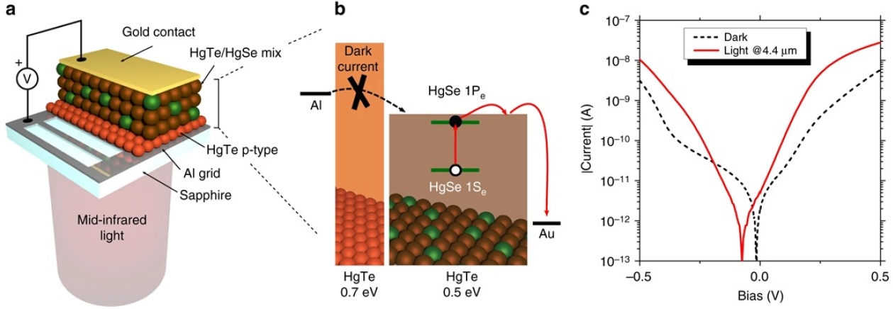
Fig. 6.(a) Schematics of the samples, PLs (b) CQDs deposited only on one DBR structure, (c) CQDs sandwiched by two DBRs without a deflector structure, and (d) CQDs sandwiched by two DBRs with a deflector structure (Adapted from Ref. [
54], licensed under CC BY 4.0)
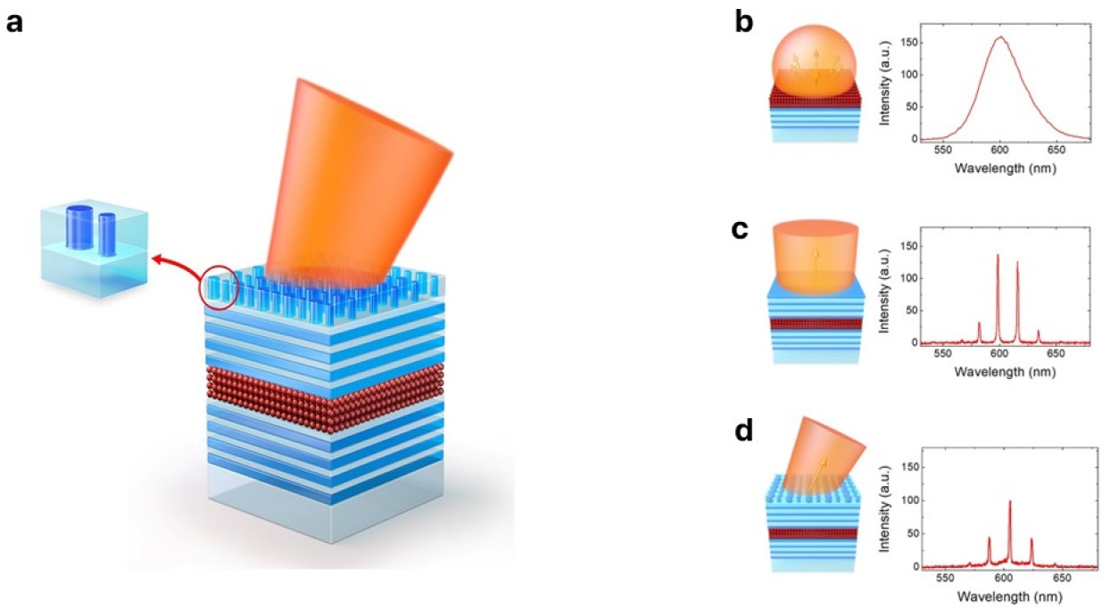
Fig. 7.Setup to study the influence of gold (Au) thin layer on the top of QD metasurfaces. (a-i) Shows the comparative impact of a gold layer on the excitation (405 nm) and emission (675 nm) process in QD metasurfaces, where w/o Au shows the S-mode and w Au the C-mode emission. (a-ii) Illustrates the first-order diffraction (C1
st) of the covering modes for lattice constants of 500 nm (green dashed line), 750 nm (pink dashed line), and 1,000 nm (blue dashed line) and its dependence on the angle of incidence (θinc). Angle-resolved photoluminescence properties of QD metasurfaces with and without a gold layer. (b) FDTD simulations and (d) experimental results of bare QD metasurfaces (“w/o Au”), contrasted with (c) simulated and (e) experimental results of QD metasurfaces with an added gold (Au) plasmonic layer. Each set shows angle-resolved photoluminescence spectroscopy across periodic structures with lattice constants of 500, 750, and 1,000 nm. The Rayleigh anomalies (RAs) of the first (1
st) and second (2
nd) orders are highlighted for both the cover (
C) and substrate (
S) regions in blue and red dashed lines, respectively. The top rows of each figure depict the dispersion without the gold layer, while the bottom rows illustrate the influence of the gold layer on the dispersion (Adapted from Ref. [
55], licensed under CC BY 4.0)
References
- 1. J. Seo, S. Kim, D. Yeo, N. Gwak, and N. Oh, Nano Convergence, 12, 26 (2025). doi: https://doi.org/10.1186/s40580-025-00489-y
- 2. M. J. Si, S. Jee, M. Yang, D. Kim, Y. Ahn, S. Lee, C. Kim, I. H. Bae, and S. W. Baek, Adv. Sci., 11, 2306798 (2024). doi: https://doi.org/10.1002/advs.202306798
- 3. Y. H. Deng, C. Pang, E. Kheradmand, J. Leemans, J. Bai, M. Minjauw, J. Liu, K. Molkens, J. Beeckman, C. Detavernier, P. Geiregat, D. Van Thourhout, and Z. Hens, Adv. Mater., 36, 2402002 (2024). doi: https://doi.org/10.1002/adma.202402002
- 4. L. Qian, X. Zhao, K. Zhang, C. Huo, Y. Li, N. Yan, F. Shi, X. Peng, and M. Chen, Nanomaterials, 15, 262 (2025). doi: https://doi.org/10.3390/nano15040262
- 5. X. Xue, Q. Hao, and M. Chen, Light Sci. Appl., 13, 89 (2024). doi: https://doi.org/10.1038/s41377-024-01436-y
- 6. Y. Jeong and G. H. Kim, J. Korean Inst. Electr. Electron. Mater. Eng., 37, 374 (2024). doi: https://doi.org/10.4313/JKEM.2024.37.4.3
- 7. G. Konstantatos and E. H. Sargent, Infrared Phys. Technol., 54, 278 (2011). doi: https://doi.org/10.1016/j.infrared.2010.12.029
- 8. Y. Zhang, M. Vafaie, J. Xu, J. M. Pina, P. Xia, A. M. Najarian, O. Atan, M. Imran, K. Xie, S. Hoogland, and E. H. Sargent, Adv. Mater., 34, 2206884 (2022). doi: https://doi.org/10.1002/adma.202206884
- 9. F. E. S. Gorris, M. Deffner, S. Priyadarshi, C. Klinke, H. Weller, and H. Lange, Adv. Opt. Mater., 8, 1901058 (2020). doi: https://doi.org/10.1002/adom.201901058
- 10. S. Zeiske, H. W. Ban, X. Li, B. Deng, R. López-Arteaga, U. H. Kazianga, M. G. Han, T. G. Kim, B. Chen, and E. H. Sargent, Nano Lett., 25, 16862 (2025). doi: https://doi.org/10.1021/acs.nanolett.5c04477
- 11. L. Peng, Y. Wang, Y. Ren, Z. Wang, P. Cao, and G. Konstantatos, ACS Nano, 18, 5113 (2024). doi: https://doi.org/10.1021/acsnano.3c12007
- 12. J. Leemans, V. Pejović, E. Georgitzikis, M. Minjauw, A. B. Siddik, Y. H. Deng, Y. Kuang, G. Roelkens, C. Detavernier, I. Lieberman, P. E. Malinowski, D. Cheyns, and Z. Hens, Adv. Sci., 9, 2200844 (2022). doi: https://doi.org/10.1002/advs.202200844
- 13. B. Sun, A. M. Najarian, L. K. Sagar, M. Biondi, M. J. Choi, X. Li, L. Levina, S. W. Baek, C. Zheng, S. Lee, A. R. Kirmani, R. Sabatini, J. Abed, M. Liu, M. Vafaie, P. Li, L. J. Richter, O. Voznyy, M. Chekini, Z. H. Lu, F. P. García de Arquer, and E. H. Sargent, Adv. Mater., 34, 2203039 (2022). doi: https://doi.org/10.1002/adma.202203039
- 14. B. K. Jung, H. K. Woo, C. Shin, T. Park, N. Li, K. J. Lee, W. Kim, J. H. Bae, J. P. Ahn, T. N. Ng, and S. J. Oh, Adv. Opt. Mater., 10, 2101611 (2022). doi: https://doi.org/10.1002/adom.202101611
- 15. H. C. V. Tran, E. Jang, J. Kim, M. Choi, Y. Park, H. Jeong, T. Goo, S. Bae, and S. Jeong, ACS Appl. Mater. Interfaces, 17, 15666 (2025). doi: https://doi.org/10.1021/acsami.4c22853
- 16. P. Liu, S. Lu, J. Liu, B. Xia, G. Yang, M. Ke, X. Zhao, J. Yang, Y. Liu, C. Ge, G. Liang, W. Chen, X. Lan, J. Zhang, L. Gao, and J. Tang, InfoMat, 6, e12497 (2024). doi: https://doi.org/10.1002/inf2.12497
- 17. Y. Tang, F. Wu, F. Chen, Y. Zhou, P. Wang, M. Long, W. Zhou, Z. Ning, J. He, F. Gong, Z. Zhu, S. Qin, and W. Hu, Small, 14, 1803158 (2018). doi: https://doi.org/10.1002/smll.201803158
- 18. Y. Wang, H. Hu, M. Yuan, H. Xia, X. Zhang, J. Liu, J. Yang, S. Xu, Z. Shi, J. He, J. Zhang, L. Gao, J. Tang, and X. Lan, ACS Appl. Mater. Interfaces, 15, 58573 (2023). doi: https://doi.org/10.1021/acsami.3c12918
- 19. S. Jeong, J. Kyhm, S. K. Cha, D. K. Hwang, B. K. Ju, J. S. Park, S. J. Kang, and I. K. Han, Small, 15, 1900008 (2019). doi: https://doi.org/10.1002/smll.201900008
- 20. V. Pejović, E. Georgitzikis, J. Lee, I. Lieberman, D. Cheyns, P. Heremans, and P. E. Malinowski, IEEE Trans. Electron Devices, 69, 2840 (2022). doi: https://doi.org/10.1109/TED.2021.3133191
- 21. J. Han, K. Huang, X. Su, X. Xiao, X. Gong, H. Wang, and J. Cao, ACS Nano, 17, 9510 (2023). doi: https://doi.org/10.1021/acsnano.3c02064
- 22. J. Luo, G. S. Selopal, X. Tong, and Z. Wang, Electron., 2, e30 (2024). doi: https://doi.org/10.1002/elt2.30
- 23. M. Chen, L. Shao, S. V. Kershaw, H. Yu, J. Wang, A. L. Rogach, and N. Zhao, ACS Nano, 8, 8208 (2014). doi: https://doi.org/10.1021/nn502510u
- 24. S. Bae, M. Duff, J. Y. Hong, and J. K. Lee, Nano Convergence, 10, 31 (2023). doi: https://doi.org/10.1186/s40580-023-00379-1
- 25. N. Đorđević, R. Schwanninger, M. Yarema, S. Koepfli, O. Yarema, Y. Salamin, N. Lassaline, B. Cheng, N. Yazdani, A. Dorodnyy, Y. M. Fedoryshyn, V. Wood, and J. Leuthold, ACS Photonics, 9, 482 (2022). doi: https://doi.org/10.1021/acsphotonics.1c01204
- 26. T. H. Dang, M. Cavallo, A. Khalili, E. Bossavit, H. Zhang, Y. Prado, C. Abadie, E. Dandeu, S. Ithurria, G. Vincent, Y. Todorov, C. Sirtori, A. Vasanelli, and E. Lhuillier, ACS Photonics, 11, 1928 (2024). doi: https://doi.org/10.1021/acsphotonics.3c01896
- 27. T. H. Dang, A. Khalili, C. Abadie, C. Gréboval, M. Cavallo, H. Zhang, E. Bossavit, J. K. Utterback, E. Dandeu, Y. Prado, G. Vincent, S. Ithurria, Y. Todorov, C. Sirtori, A. Vasanelli, and E. Lhuillier, ACS Photonics, 9, 2528 (2022). doi: https://doi.org/10.1021/acsphotonics.2c00738
- 28. A. Caillas, S. Suffit, P. Filloux, E. Lhuillier, and A. Degiron, Nano Lett., 22, 2155 (2022). doi: https://doi.org/10.1021/acs.nanolett.1c03865
- 29. J. Tong, F. Suo, L. Y. M. Tobing, N. Yao, D. Zhang, Z. Huang, and D. H. Zhang, ACS Appl. Mater. Interfaces, 12, 8835 (2020). doi: https://doi.org/10.1021/acsami.9b19187
- 30. A. Yakimov, V. Kirienko, A. Bloshkin, D. Utkin, and A. Dvurechenskii, Phys. Status Solidi A, 222, e202500606 (2025). doi: https://doi.org/10.1002/pssa.202500606
- 31. W. Wang, X. Yang, T. S. Luk, and J. Gao, Appl. Phys. Lett., 114, 021103 (2019). doi: https://doi.org/10.1063/1.5081688
- 32. Q. Xu, L. Meng, K. Sinha, F. I. Chowdhury, J. Hu, and X. Wang, ACS Photonics, 7, 1297 (2020). doi: https://doi.org/10.1021/acsphotonics.0c00363
- 33. M. Chen, L. Lu, H. Yu, C. Li, and N. Zhao, Adv. Sci., 8, 2101560 (2021). doi: https://doi.org/10.1002/advs.202101560
- 34. R. Schwanninger, S. M. Koepfli, O. Yarema, A. Dorodnyy, M. Yarema, A. Moser, S. Nashashibi, Y. Fedoryshyn, V. Wood, and J. Leuthold, ACS Appl. Mater. Interfaces, 15, 10847 (2023). doi: https://doi.org/10.1021/acsami.2c23050
- 35. M. H. Lee, S. Kim, S. J. Hong, M. S. Kim, H. Kim, and J. Y. Lee, J. Flex. Print. Electron., 3, 221 (2024). doi: https://doi.org/10.56767/jfpe.2024.3.2.221
- 36. I. Staude and J. Schilling, Nat. Photon., 11, 274 (2017). doi: https://doi.org/10.1038/nphoton.2017.39
- 37. S. Jiang, X. Liu, J. Liu, D. Ye, Y. Duan, K. Li, Z. Yin, and Y. Huang, Adv. Mater., 34, 2200070 (2022). doi: https://doi.org/10.1002/adma.202200070
- 38. N. I. Zheludev and Y. S. Kivshar, Nat. Mater., 11, 917 (2012). doi: https://doi.org/10.1038/nmat3431
- 39. S. Wang, P. C. Wu, V. C. Su, Y. C. Lai, C. H. Chu, J. W. Chen, S. H. Lu, J. Chen, B. Xu, C. H. Kuan, T. Li, S. Zhu, and D. P. Tsai, Nat. Commun., 8, 187 (2017). doi: https://doi.org/10.1038/s41467-017-00166-7
- 40. L. Feng, P. Huo, Y. Liang, and T. Xu, Adv. Mater., 32, 1903787 (2020). doi: https://doi.org/10.1002/adma.201903787
- 41. F. Yang, R. H. Li, S. L. Tan, J. W. Dong, and S. J. Jiang, Nanophotonics, 12, 2451 (2023). doi: https://doi.org/10.1515/nanoph-2023-0021
- 42. Y. Zhao and A. Alù, Phys. Rev. B, 84, 205428 (2011). doi: https://doi.org/10.1103/PhysRevB.84.205428
- 43. D. Wen, F. Yue, C. Zhang, X. Zang, H. Liu, W. Wang, and X. Chen, Appl. Phys. Lett., 111, 023102 (2017). doi: https://doi.org/10.1063/1.4993429
- 44. N. Ullah, R. Zhao, and L. Huang, Micromachines, 13, 1025 (2022). doi: https://doi.org/10.3390/mi13071025
- 45. S. W. Moon, Y. Kim, G. Yoon, and J. Rho, iScience, 23, 101877 (2020). doi: https://doi.org/10.1016/j.isci.2020.101877
- 46. I. Kim, G. Yoon, J. Jang, P. Genevet, K. T. Nam, and J. Rho, ACS Photonics, 5, 3876 (2018). doi: https://doi.org/10.1021/acsphotonics.8b00809
- 47. W. Wan, J. Gao, and X. Yang, ACS Nano, 10, 10671 (2016). doi: https://doi.org/10.1021/acsnano.6b05453
- 48. B. K. Jung, T. Park, Y. K. Choi, Y. M. Lee, T. H. Kim, B. Seo, S. Oh, J. W. Shim, Y. H. Lo, T. N. Ng, and S. J. Oh, Nanoscale Horiz., 9, 487 (2024). doi: https://doi.org/10.1039/D3NH00456B
- 49. Y. Yifat, M. Ackerman, and P. Guyot-Sionnest, Appl. Phys. Lett., 110, 041106 (2017). doi: https://doi.org/10.1063/1.4975058
- 50. R. Schwanninger, S. Nashashibi, O. Yarema, S. M. Koepfli, Y. Fedoryshyn, V. Wood, and J. Leuthold, Adv. Opt. Mater., 12, 2303223 (2024). doi: https://doi.org/10.1002/adom.202303223
- 51. C. Livache, B. Martinez, N. Goubet, C. Gréboval, J. Qu, A. Chu, S. Royer, S. Ithurria, M. G. Silly, B. Dubertret, and E. Lhuillier, Nat. Commun., 10, 2125 (2019). doi: https://doi.org/10.1038/s41467-019-10170-8
- 52. T. Chung, H. Wang, and H. Cai, Nanotechnol., 34, 402001 (2023). doi: https://doi.org/10.1088/1361-6528/ace117
- 53. B. García García, M. G. Fernández-Manteca, D. C. Zografopoulos, C. Gómez-Galdós, A. A. Ocampo-Sosa, L. Rodríguez-Cobo, J. F. Algorri, and A. Cobo, Biosens.-Basel, 15, 401 (2025). doi: https://doi.org/10.3390/bios15070401
- 54. Y. Park, H. Kim, J. Y. Lee, W. Ko, K. Bae, and K. S. Cho, Nanophotonics, 9, 1023 (2020). doi: https://doi.org/10.1515/nanoph-2020-0158
- 55. M. Adnan, S. Sarkar, O. Aftenieva, J. Brunner, A. Fery, Y. Vaynzof, and T. A. F. König, Adv. Opt. Mater., 13, 2403397 (2025). doi: https://doi.org/10.1002/adom.202403397
- 56. J. Liu and R. Paiella, Opt. Lett., 49, 1417 (2024). doi: https://doi.org/10.1364/OL.509642