ABSTRACT
Wearable temperature sensors are becoming increasingly important for continuous health monitoring, personalized healthcare, and biointegrated electronic systems. However, conventional temperature-sensing platforms often suffer from limited thermal sensitivity, insufficient mechanical compliance, and unstable performance under repeated deformation, making it difficult to detect subtle physiological temperature variations in real time. Here, this tutorial status report presents a fabrication strategy for highly sensitive wearable temperature sensors based on gold-doped crystalline silicon nanomembranes. Gold diffusion into crystalline silicon introduces deep-level impurity states that modulate the Fermi level and shift the freeze-out region toward the physiological temperature range, enabling an ultrahigh negative temperature coefficient of resistance. By integrating the gold-doped silicon nanomembrane with a polyimide-supported ultrathin platform, neutral mechanical plane design, and serpentine mesh interconnects, the resulting device can provide high thermal sensitivity, fast response, conformal skin attachment, and stable operation under mechanical deformation. This fabrication approach is expected to broaden the use of impurity-engineered silicon nanomembranes in next-generation wearable sensors, flexible bioelectronics, and multifunctional healthcare monitoring systems.
-
KEYWORDS: Gold-doped silicon nanomembrane, Wearable temperature sensor, Flexible bioelectronics, Temperature coefficient of resistance, Transfer printing
1 Introduction
■ Wearable temperature sensors have become important components in continuous health monitoring, personalized medicine, sports healthcare, and biointegrated electronic systems.
■ Body temperature is closely related to physiological conditions such as inflammation, infection, cardiovascular activity, respiratory function, wound healing, and metabolic changes.
■ Conventional temperature sensors based on metals or organic materials have been widely used, but they still face limitations in detecting subtle temperature changes with high sensitivity and long-term reliability [
1–
3].
• Metal-based resistance temperature sensors generally show stable electrical behavior, but their temperature coefficient of resistance is relatively low.
• Organic temperature-sensitive materials provide mechanical softness, but they may suffer from slow response, environmental instability, and limited long-term durability.
• Therefore, a new sensing platform that simultaneously provides high thermal sensitivity, mechanical flexibility, fast response, and stable operation is required.
■ Crystalline silicon is one of the most reliable inorganic semiconductor materials and has been widely used in electronic devices, sensors, and integrated circuits.
■ However, bulk silicon is mechanically rigid and brittle, which makes it difficult to directly integrate with soft and curvilinear biological surfaces.
■ Silicon nanomembranes provide an effective strategy to overcome this limitation because ultrathin silicon can maintain the intrinsic electronic properties of crystalline silicon while gaining mechanical flexibility.
• When the thickness of silicon is reduced to the nanometer scale, its bending stiffness is significantly decreased.
• This allows silicon to conformally contact soft surfaces such as human skin.
• In addition, silicon nanomembranes can be patterned and integrated using conventional semiconductor microfabriccation processes.
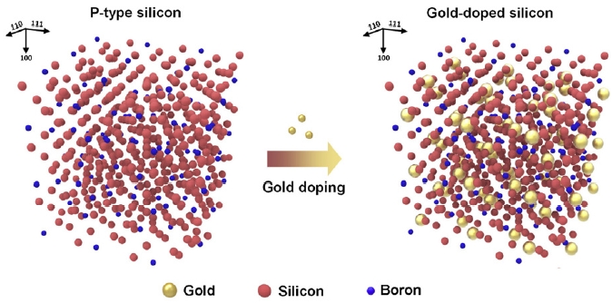
■ Gold doping is an effective method for modulating the electrical and thermal properties of silicon.
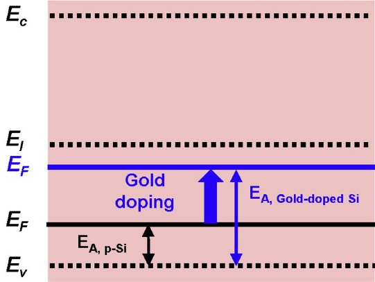
■ Gold atoms act as deep-level impurities in silicon and can shift the Fermi level by compensating free carriers.
■ This impurity-induced electronic modulation can shift the freeze-out region of silicon toward the physiological temperature range, resulting in an ultrahigh negative temperature coefficient of resistance.
■ This tutorial status report introduces the fabrication process of a gold-doped crystalline silicon nanomembrane-based wearable temperature sensor.
■ The overall process includes SOI wafer preparation, gold deposition, high-temperature diffusion, silicon nanomembrane release, transfer printing, device patterning, metallization, encapsulation, and wearable integration.
■ This paper aims to provide practical guidelines for fabricating highly sensitive semiconductor-based wearable temperature sensors and to discuss their potential applications in flexible bioelectronics and healthcare monitoring systems [
4–
6].
2 Principle of Gold-Doped Silicon Nanomembrane Temperature Sensors
2.1 Temperature-Dependent Resistance of Silicon
■ The resistance of silicon is determined by carrier concentration and carrier mobility.
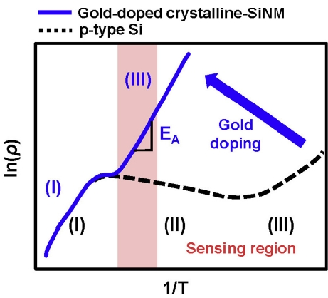
■ In doped silicon, the temperature-dependent resistance behavior can generally be divided into three regions: freezeout region, extrinsic region, and intrinsic region.
• In the freeze-out region, dopants are not fully ionized, and carrier concentration is strongly affected by temperature.
• In the extrinsic region, most dopants are ionized, and the resistance change is relatively moderate.
• In the intrinsic region, thermally generated electron–hole pairs dominate the electrical conduction.
■ For temperature sensing applications, it is advantageous to locate the most temperature-sensitive region near the target temperature range.
■ However, conventional silicon does not naturally show its highest thermal sensitivity near the physiological temperature range.
■ Therefore, impurity engineering is required to modulate the electronic structure of silicon and enhance its resistance change near room and body temperatures.
2.2 Gold as a Deep-Level Impurity in Silicon
■ Gold is a representative deep-level impurity in silicon.
■ Unlike shallow dopants such as boron, phosphorus, or arsenic, gold introduces deep energy levels within the silicon bandgap.
■ During high-temperature annealing, gold atoms diffuse into silicon through mechanisms such as the kick-out mechanism and the Frank–Turnbull mechanism.
■ Diffused gold atoms compensate free carriers and shift the Fermi level toward the intrinsic energy level.
• In p-type silicon, gold can compensate acceptor-induced holes.
• In n-type silicon, gold can compensate donor-induced electrons.
• This carrier compensation increases silicon resistivity and strongly modifies the temperature-dependent resistance behavior.
■ As a result, the freeze-out region can be shifted toward the physiological temperature range.
■ When temperature increases, the carrier concentration increases significantly, while the resistance decreases.
■ Therefore, gold-doped silicon exhibits a large negative temperature coefficient of resistance.
2.3 Advantage of Silicon Nanomembrane Geometry
■ Although crystalline silicon has excellent electrical reliability, bulk silicon is not suitable for wearable applications because of its high stiffness.
■ Silicon nanomembranes overcome this limitation by reducing the silicon thickness to the nanoscale.
■ The ultrathin geometry dramatically decreases bending stiffness and allows silicon to be integrated onto flexible polymer substrates.
• Silicon nanomembranes can conform to curved surfaces.
• They can maintain crystalline semiconductor properties.
• They are compatible with photolithography, dry etching, metallization, and transfer printing.
■ Therefore, silicon nanomembranes provide a bridge between high-performance semiconductor materials and mechanically soft wearable devices.
■ In the gold-doped silicon nanomembrane platform, thermal sensitivity is improved by gold doping, while mechanical compliance is achieved through the ultrathin silicon geometry.
3 Overall Fabrication Strategy
■ The fabrication of the gold-doped silicon nanomembranebased wearable temperature sensor consists of four major steps.
• Preparation of gold-doped silicon nanomembranes from an SOI wafer.
• Transfer of the released silicon nanomembrane onto a flexible polymer substrate.
• Patterning of the sensing region and formation of metal interconnects.
• Encapsulation, mesh structure definition, and wearable integration.
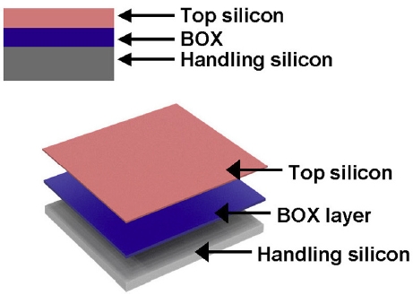
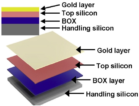
■ The process starts from a silicon-on-insulator wafer because the top silicon layer can be used as the active sensing material.
■ The buried oxide layer serves as a sacrificial layer that enables the release of the silicon nanomembrane.
■ Gold is deposited on the top silicon layer and diffused into silicon through high-temperature annealing.
■ After gold diffusion, the gold-doped silicon nanomembrane is released by selectively removing the buried oxide layer.
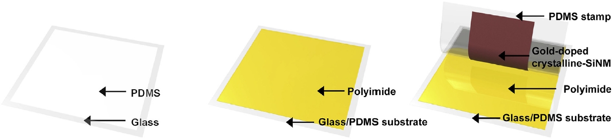
■ The released nanomembrane is transferred onto a polyimidecoated flexible substrate using a PDMS stamp.
■ The transferred nanomembrane is then patterned into a temperature-sensing geometry through photolithography and dry etching.
■ Metal electrodes and serpentine interconnects are formed to provide stable electrical readout under mechanical deformation.
■ Finally, the device is encapsulated with polyimide and defined into an ultrathin mesh structure for conformal skin attachment.
4 Preparation of Gold-Doped Silicon Nanomembrane
4.1 SOI Wafer Preparation
■ An SOI wafer is used as the starting substrate for fabricating the silicon nanomembrane.
■ The top silicon layer functions as the active temperaturesensing material.
■ The buried oxide layer functions as a sacrificial layer for nanomembrane release.
■ Before gold deposition, the SOI wafer should be cleaned to remove organic contaminants, particles, and native oxide.
• Piranha cleaning can be used to remove organic residues.
• Deionized water rinsing is required to eliminate residual chemicals.
• Buffered oxide etchant can be used to remove native oxide from the silicon surface.
■ After oxide removal, the silicon surface becomes hydrophobic and can be easily reoxidized.
■ Therefore, gold deposition should be performed immediately after the oxide removal step.
■ Chemical cleaning and etching processes should be performed with proper safety procedures because piranha solution and hydrofluoric acid-based etchants are highly hazardous.
4.2 Gold Thin-Film Deposition
■ A thin gold layer is deposited on the cleaned top silicon surface.
■ Thermal evaporation can be used to form a uniform gold film with controlled thickness.
■ The gold layer serves as the diffusion source during the subsequent high-temperature annealing process.
■ The thickness of the gold layer is an important parameter because it affects the final gold concentration in silicon.
• Excessively thin gold may result in insufficient carrier compensation.
• Excessively thick gold may cause nonuniform diffusion or excessive contamination.
• A carefully controlled gold thickness is therefore required for reproducible sensor performance.
■ The evaporation chamber should reach a high-vacuum condition before deposition.
■ A clean and uniform gold film is necessary to obtain uniform thermal sensitivity across the silicon nanomembrane.
4.3 High-Temperature Gold Diffusion
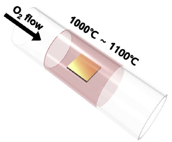
■ Gold diffusion into silicon is performed by high-temperature annealing.
■ The annealing temperature should be sufficiently high to allow gold atoms to diffuse into the crystalline silicon layer.
■ During annealing, gold atoms diffuse from the deposited gold film into silicon and form deep-level impurity states.
■ These deep-level states modulate the Fermi level and alter the carrier activation behavior of silicon.
■ A dedicated quartz tube is strongly recommended for gold diffusion.
• Gold contamination can seriously affect other silicon devices.
• The gold-doping furnace should therefore be separated from general semiconductor processing furnaces.
• This is especially important in shared cleanroom environments
■ After annealing, oxide formed on the silicon surface should be removed using hydrofluoric acid-based etching.
■ The wafer should then be rinsed and dried carefully before the nanomembrane release process.
5 Release and Transfer of Gold-Doped Silicon Nanomembrane
5.1 Formation of Etching Access Holes
■ To release the gold-doped silicon nanomembrane, the buried oxide layer must be selectively removed.
■ Etching access holes can be formed in the top silicon layer to allow the etchant to reach the buried oxide layer.
■ Photolithography is used to define the hole pattern.
■ Reactive ion etching is then used to etch the exposed silicon regions.
■ The hole pattern should be designed to promote uniform buried oxide removal while maintaining the mechanical integrity of the silicon nanomembrane.
• If the hole density is too low, oxide etching may be slow and incomplete.
• If the hole density is too high, the silicon nanomembrane may become fragile.
• Therefore, hole size, spacing, and distribution should be optimized.
5.2 Release of the Silicon Nanomembrane
■ The buried oxide layer is selectively etched using hydrofluoric acid-based solution.
■ As the buried oxide layer is removed, the top gold-doped silicon layer becomes released from the handle wafer.
■ The released silicon nanomembrane is extremely thin and fragile.
■ Therefore, the etching time, rinsing process, and drying process should be carefully controlled.
■ Incomplete etching may prevent successful pickup of the silicon nanomembrane.
■ Excessive etching or mechanical disturbance may cause tearing, folding, or cracking of the nanomembrane.
■ A stable release process is essential for achieving high device yield.
5.3 PDMS-Assisted Transfer Printing
■ A PDMS stamp is used to pick up the released gold-doped silicon nanomembrane.
■ PDMS is suitable for transfer printing because it is soft, conformable, and capable of reversible adhesion.
■ The PDMS stamp should make uniform contact with the released silicon nanomembrane.
■ Gradual contact from one edge to the opposite side can help reduce trapped air bubbles.
■ After full contact is achieved, the PDMS stamp is peeled away to retrieve the silicon nanomembrane.
• Contact pressure should be carefully controlled.
• Peeling speed can influence transfer yield.
• Nonuniform contact may generate wrinkles or cracks.
■ Successful transfer printing requires proper control of adhesion between the silicon nanomembrane, donor wafer, and PDMS stamp.
6 Flexible Substrate Preparation and Nanomembrane Transfer
6.1 Polyimide-Coated Temporary Substrate
■ A flexible substrate is prepared using polyimide on a temporary carrier.
■ A glass substrate coated with PDMS can be used as a temporary support.
■ Polyimide is spin-coated on the PDMS-coated glass substrate.
■ The polyimide layer provides mechanical support, thermal stability, and process compatibility.
■ Surface treatment such as UV ozone or oxygen plasma can improve wetting and adhesion before polyimide coating.
■ The thickness of the polyimide layer should be selected considering flexibility, mechanical reliability, and neutral mechanical plane design.
6.2 Transfer of Gold-Doped Silicon Nanomembrane onto Polyimide
■ The PDMS stamp carrying the gold-doped silicon nanomembrane is laminated onto the polyimide-coated substrate.
■ Mild thermal treatment can improve adhesion between the silicon nanomembrane and polyimide.
■ The PDMS stamp is then peeled away, leaving the gold-doped silicon nanomembrane on the flexible substrate.
■ Uniform attachment of the silicon nanomembrane is critical for subsequent photolithography and device patterning.
■ Wrinkles, cracks, and trapped air bubbles should be minimized during transfer.
■ After transfer, additional curing can be performed to stabilize the polyimide substrate.
7 Device Patterning and Metallization
7.1 Patterning of the Sensing Region
■ The transferred gold-doped silicon nanomembrane is patterned into the desired temperature-sensing geometry.
■ Photolithography is used to define the sensor pattern.
■ Reactive ion etching is used to remove unnecessary silicon regions.
■ The sensing geometry determines the electrical resistance, spatial resolution, and mechanical robustness of the device.
• A narrow and long sensing line can increase resistance and sensitivity.
• A compact geometry can improve spatial resolution.
• The pattern should also avoid excessive stress concentration.
■ The sensing region should be designed to maintain stable resistance during bending and stretching.
7.2 Metal Electrode and Interconnect Formation
■ Metal electrodes are formed to electrically connect the golddoped silicon nanomembrane sensor to external measurement systems.
■ Before metallization, native oxide on the contact region should be removed to reduce contact resistance.
■ A thin adhesion layer such as chromium can be deposited before gold deposition.
■ Gold is commonly used as the main electrode material because of its high conductivity and chemical stability.
■ Lift-off is performed after metal deposition to define the electrode and interconnect patterns.
■ Stable metal–silicon contact is essential for reliable temperature measurement.
■ Poor contact can cause unstable resistance, signal drift, and increased noise.
7.3 Serpentine Interconnect Design
■ Serpentine interconnects are used to improve mechanical stretchability.
■ Straight metal lines can easily crack under tensile strain.
■ In contrast, serpentine interconnects can unfold and deform under stretching.
■ This geometry reduces strain concentration in the active sensing region.
■ The sensing island and serpentine interconnects perform different mechanical roles.
• The sensing island maintains stable temperature measurement.
• The serpentine interconnect accommodates external deformation.
• The mesh layout improves breathability and skin compatibility.
■ This structural design is important for wearable applications where the device is continuously exposed to body motion.
8 Encapsulation and Neutral Mechanical Plane Design
8.1 Polyimide Encapsulation
■ After metallization, the device is encapsulated with an additional polyimide layer.
■ The encapsulation layer protects the silicon nanomembrane and metal interconnects from environmental exposure.
■ It also improves mechanical durability during handling and wearable operation.
■ Encapsulation can protect the device from sweat, moisture, particles, and mechanical damage.
■ The encapsulation layer should be thin enough to maintain flexibility but thick enough to provide protection.
8.2 Neutral Mechanical Plane Design
■ The neutral mechanical plane is the position in a multilayer structure where bending-induced strain becomes nearly zero.
■ Placing the gold-doped silicon nanomembrane near the neutral mechanical plane reduces strain applied to the sensing material.
■ This design is important because silicon has piezoresistive properties.
■ Without proper mechanical design, deformation-induced resistance changes may interfere with temperature sensing.
■ By locating the silicon nanomembrane near the neutral mechanical plane, the device can maintain accurate temperature measurement during bending.
■ Therefore, neutral mechanical plane design improves both mechanical reliability and sensing accuracy.
9 Wearable Integration and Operation
9.1 Mesh-Structured Device Release
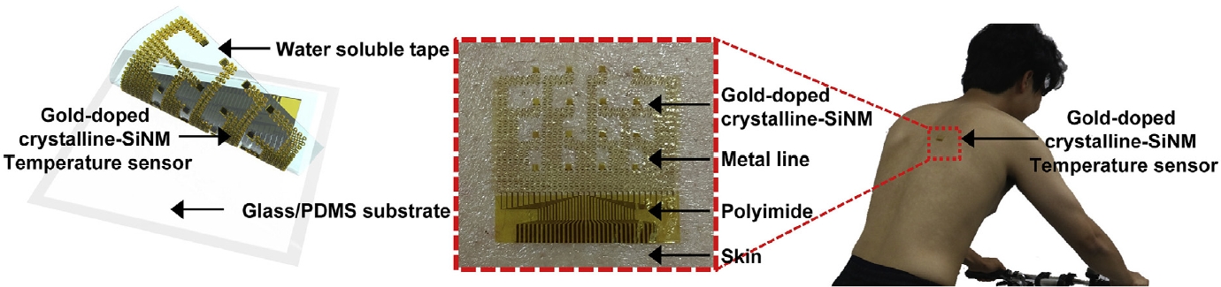
■ After encapsulation, the entire device is patterned into a mesh structure.
■ The mesh design improves flexibility, stretchability, and skin compatibility.
■ Open spaces in the mesh allow sweat and air to pass through.
■ This helps reduce discomfort during long-term skin attachment.
■ The final device is released from the temporary substrate using a transfer support such as water-soluble tape.
■ Because the device is ultrathin, careful handling is required during release and transfer.
9.2 Conformal Attachment to Skin
■ The released device can be laminated onto the skin or another soft biological surface.
■ The ultrathin structure allows conformal contact with curvilinear skin surfaces.
■ Strong conformal contact reduces air gaps between the sensor and skin.
■ This improves thermal coupling and enhances the accuracy of temperature measurement.
■ The device can adhere to the skin through van der Waals forces without requiring thick adhesive layers.
■ This adhesive-free or minimally adhesive attachment can reduce skin irritation and improve user comfort.
9.3 Continuous Temperature Monitoring
■ The resistance of the gold-doped silicon nanomembrane changes in response to temperature variation.
■ By measuring resistance in real time, continuous temperature monitoring can be achieved.
■ The high negative temperature coefficient of resistance enables detection of subtle thermal changes.
■ The fast response of the ultrathin device allows dynamic monitoring of rapid temperature fluctuations.
■ The device can be used for skin temperature monitoring, respiration monitoring, exercise tracking, and localized thermal mapping.
10 Performance Considerations
10.1 Thermal Sensitivity
■ The most important performance parameter of a resistancebased temperature sensor is the temperature coefficient of resistance.
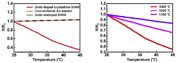
■ Gold-doped silicon nanomembranes can show an ultrahigh negative temperature coefficient of resistance.
■ This high thermal sensitivity originates from gold-induced deep-level impurity states and carrier compensation.
■ Compared with conventional metal-based temperature sensors, the gold-doped silicon nanomembrane platform can detect much smaller temperature variations.
■ This characteristic is particularly useful for physiological temperature monitoring, where temperature changes are often small and localized.
10.2 Response Time
■ Response time is another important parameter for real-time monitoring.
■ The ultrathin silicon nanomembrane and polymer substrate reduce the thermal mass of the device.
■ Low thermal mass enables rapid heat transfer between the skin and the sensing material.
■ Therefore, the device can respond quickly to dynamic temperature changes. Fast response is useful for monitoring respiration, exerciseinduced thermal changes, and transient physiological events.
10.3 Mechanical Stability
■ Mechanical stability is essential for wearable devices because they are repeatedly exposed to bending, stretching, and twisting.
■ The gold-doped silicon nanomembrane-based sensor uses several mechanical design strategies.
• Ultrathin silicon reduces bending stiffness.
• Neutral mechanical plane design minimizes strain in the sensing layer.
• Serpentine interconnects accommodate stretching.
• Mesh architecture improves conformability and breathability.
■ These strategies allow the device to maintain stable electrical performance under mechanical deformation.
11 Applications
11.1 Continuous Healthcare Monitoring
■ The gold-doped silicon nanomembrane temperature sensor can be used for continuous body temperature monitoring.
■ Such monitoring is useful for fever detection, inflammation tracking, wound healing assessment, and personalized healthcare.
■ The high sensitivity of the sensor allows detection of small changes in skin temperature.
■ The conformal and ultrathin device structure enables longterm attachment with reduced discomfort.
11.2 Respiration Monitoring
■ Respiration can be monitored by detecting temperature changes near the nose or mouth.
■ Exhaled air increases local temperature, while inhaled air causes cooling.
■ A fast and sensitive temperature sensor can detect these cyclic thermal signals.
■ Therefore, the gold-doped silicon nanomembrane sensor can be used to monitor breathing patterns in real time.
11.3 Sports and Exercise Monitoring
■ During exercise, skin temperature changes due to metabolic heat generation, blood flow variation, sweating, and environmental conditions.
■ Wearable temperature sensors can provide useful information for sports performance analysis and heat stress prevention.
■ The stretchable mesh design is advantageous for sports applications because it can tolerate body motion.
■ Integration with wireless electronics could enable real-time feedback during training or rehabilitation.
11.4 Biointegrated and Implantable Electronics
■ The gold-doped silicon nanomembrane platform can also be extended to biointegrated and implantable electronics.
■ Local temperature monitoring may be useful for evaluating tissue inflammation, stimulation-induced heating, and implant safety.
■ Silicon nanomembranes can be integrated with flexible neural interfaces, cardiac sensors, and multifunctional bioelectronic systems.
■ Therefore, this platform has potential beyond skin-mounted wearable sensors.
12 Process Challenges and Limitations
■ The fabrication process requires high-temperature gold diffusion above 1,000℃.
■ This process must be performed before transfer to polymer substrates because most flexible polymers cannot withstand such high temperatures.
■ Gold contamination is another important issue in semiconductor processing.
• Gold is a deep-level impurity and can degrade the performance of conventional silicon devices.
• Dedicated process tools and quartz tubes are recommended.
• Cross-contamination should be carefully prevented.
■ Transfer printing of ultrathin silicon nanomembranes can limit fabrication yield.
■ Wrinkles, cracks, incomplete pickup, or air bubbles may occur during the transfer process.
■ Large-area fabrication requires further optimization of adhesion, stamp design, and transfer conditions.
■ Long-term wearable reliability should also be evaluated under realistic conditions such as sweat exposure, repeated movement, washing, and prolonged skin contact.
13 Future Perspectives
■ Gold-doped silicon nanomembranes provide a promising platform for next-generation wearable and biointegrated sensors.
■ The gold doping condition can be further optimized to tune the target temperature range and sensitivity.
■ High-density temperature sensor arrays can be developed for spatial thermal mapping.
■ Integration with wireless communication modules can enable remote and continuous healthcare monitoring.
■ Multimodal sensing platforms can be realized by combining temperature sensors with strain, pressure, electrophysiological, biochemical, or optical sensors.
■ The concept of impurity-engineered silicon nanomembranes can also be extended to other flexible semiconductor devices.
■ Therefore, gold-doped silicon nanomembranes represent not only a temperature-sensing platform but also a broader material-engineering strategy for high-performance flexible electronics.
14 Conclusion
■ This tutorial status report summarized the fabrication process of gold-doped crystalline silicon nanomembrane-based wearable temperature sensors.
■ Gold doping introduces deep-level impurity states in silicon, modulates the Fermi level, and shifts the freeze-out region toward the physiological temperature range.
■ This electronic modulation enables an ultrahigh negative temperature coefficient of resistance.
■ The silicon nanomembrane geometry provides mechanical flexibility while preserving the electrical advantages of crystalline silicon.
■ Polyimide encapsulation, neutral mechanical plane design, and serpentine mesh interconnects further improve mechanical reliability and wearable compatibility.
■ The fabrication process includes SOI wafer preparation, gold deposition, high-temperature diffusion, silicon nanomembrane release, PDMS-assisted transfer printing, device patterning, metallization, encapsulation, mesh definition, and skin transfer.
■ Although several challenges remain, including large-area transfer yield, gold contamination control, and long-term wearable reliability, this platform provides a promising route toward high-performance semiconductor-based wearable temperature sensors.
■ This approach is expected to contribute to future developments in flexible bioelectronics, personalized healthcare monitoring, sports wearable systems, and multifunctional biointegrated devices.
Notes
-
Acknowledgement
This work acknowledges the support received from National Research Foundation of Korea (NRF) Grant funded by the Korea government (MSIT) (RS-2025-23523363).
-
Conflict of Interest
The authors have no conflicts of interest to declare.
-
Author Contributions
Mingyu Sang: Conceptualization, Methodology, Validation, Formal analysis, Investigation, Resources, Data Curation, Writing - Original Draft, Writing - Review & Editing, Visualization, Supervision, Project administration, Funding acquisition.
Data Availability
Data derived from public domain resources.
Fig. 1.Schematic illustration of gold doping in p-type crystalline silicon
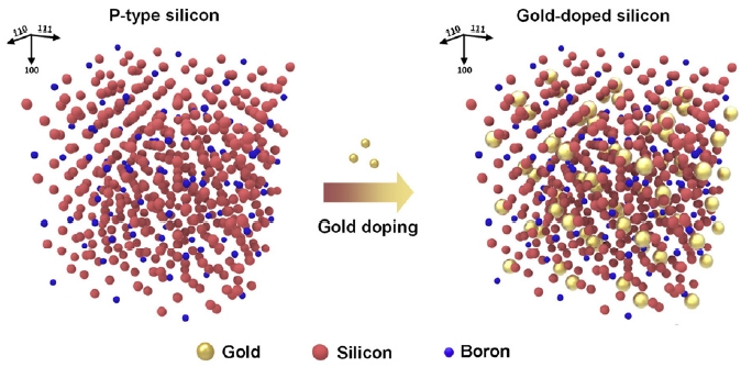
Fig. 2.Temperature-dependent resistance behavior of gold-doped crystalline silicon nanomembranes
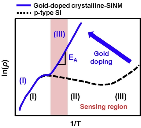
Fig. 3.Energy-band modulation of silicon induced by gold deeplevel impurity states
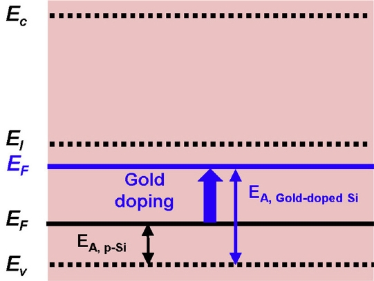
Fig. 4.Structure of the silicon-on-insulator wafer used for silicon nanomembrane fabrication
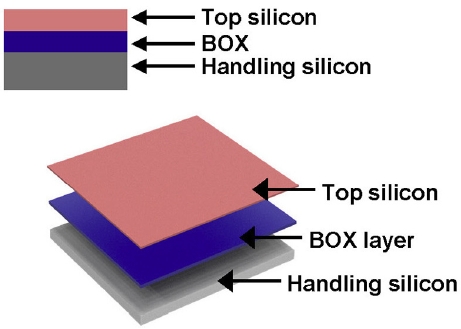
Fig. 5.Gold thin-film deposition on the top silicon layer of the SOI wafer
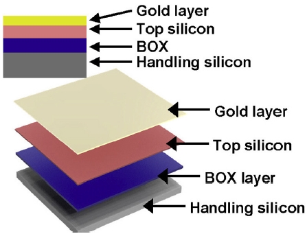
Fig. 6.High-temperature diffusion process for introducing gold atoms into crystalline silicon
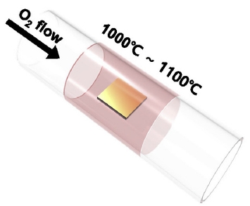
Fig. 7.Transfer of the gold-doped silicon nanomembrane onto a polyimide-coated flexible substrate
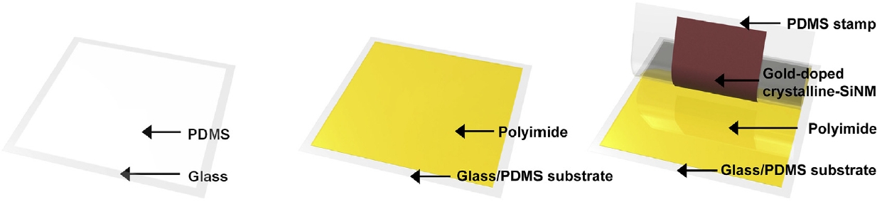
Fig. 8.Device patterning, metallization, and mesh-structured interconnect formation

Fig. 9.Wearable integration of the gold-doped silicon nanomembrane temperature sensor on skin
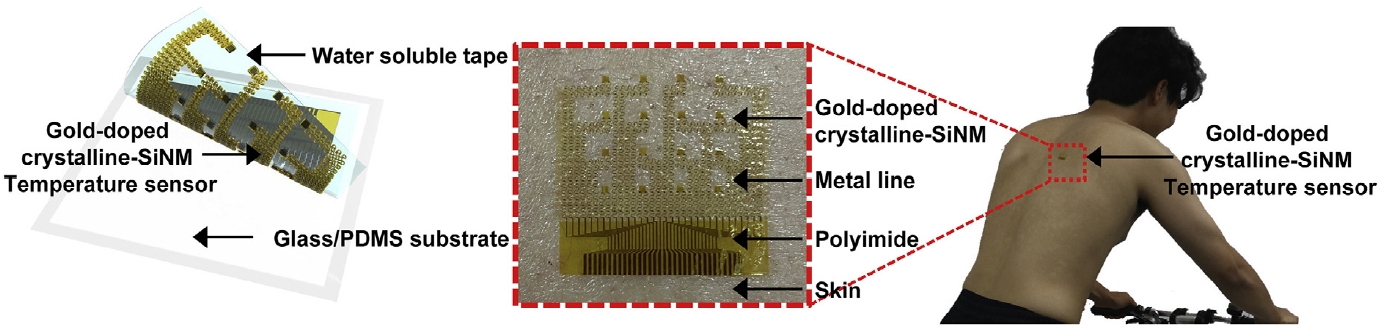
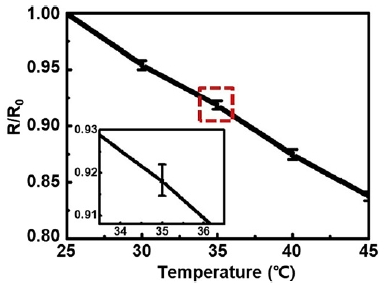
Fig. 10.Thermal sensitivity of the gold-doped silicon nanomembrane temperature sensor
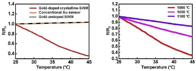
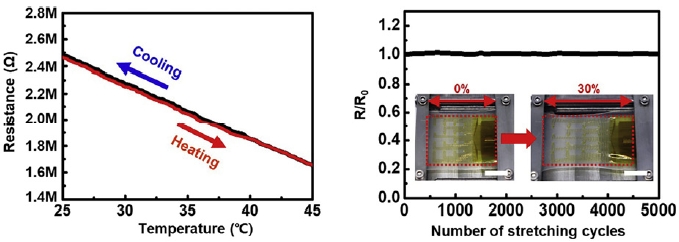
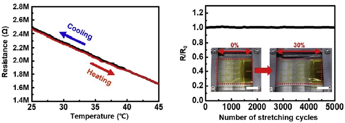
Fig. 11.Resistance response of the sensor under temperature variation
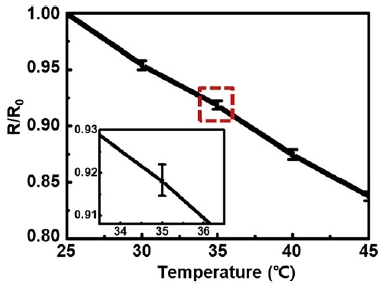
Fig. 12.Mechanical stability of the sensor under repeated stretching cycles
References
- 1. R. C. Webb, A. P. Bonifas, A. Behnaz, Y. Zhang, K. J. Yu, H. Cheng, M. Shi, Z. Bian, Z. Liu, Y. S. Kim, W. H. Yeo, J. S. Park, J. Song, Y. Li, Y. Huang, A. M. Gorbach, and J. A. Rogers, Nat. Mater., 12, 938 (2013). doi: https://doi.org/10.1038/nmat3755
- 2. J. W. Lee, R. Xu, S. Lee, K. I. Jang, Y. Yang, A. Banks, K. J. Yu, J. Kim, S. Xu, S. Ma, S. W. Jang, P. Won, Y. Li, B. H. Kim, J. Y. Choe, S. Huh, Y. H. Kwon, Y. Huang, U. Paik, and J. A. Rogers, Proc. Natl. Acad. Sci. U.S.A., 113, 6131 (2016). doi: https://doi.org/10.1073/pnas.1605720113
- 3. J. Shin, B. Jeong, J. Kim, V. B. Nam, Y. Yoon, J. Jung, S. Hong, H. Lee, H. Eom, J. Yeo, J. Choi, D. Lee, and S. H. Ko, Adv. Mater., 32, 1905527 (2020). doi: https://doi.org/10.1002/adma.201905527
- 4. C. B. Collins, R. O. Carlson, and C. J. Gallagher, Phys. Rev., 105, 1168 (1957). doi: https://doi.org/10.1103/PhysRev.105.1168
- 5. W. M. Bullis and F. J. Strieter, J. Appl. Phys., 39, 314 (1968). doi: https://doi.org/10.1063/1.1655751
- 6. J. P. Mailoa, A. J. Akey, C. B. Simmons, D. Hutchinson, J. Mathews, J. T. Sullivan, D. Recht, M. T. Winkler, J. S. Williams, J. M. Warrender, P. D. Persans, M. J. Aziz, and T. Buonassisi, Nat. Commun., 5, 3011 (2014). doi: https://doi.org/10.1038/ncomms4011